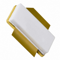
BLF6G10LS-135R,112 NXP Semiconductors, BLF6G10LS-135R,112 Datasheet - Page 38

BLF6G10LS-135R,112
Manufacturer Part Number
BLF6G10LS-135R,112
Description
IC BASESTATION FINAL SOT502B
Manufacturer
NXP Semiconductors
Datasheets
1.BLF6G20LS-140118.pdf
(100 pages)
2.BLF6G20LS-140112.pdf
(110 pages)
3.BLF6G10LS-135R112.pdf
(10 pages)
Specifications of BLF6G10LS-135R,112
Package / Case
SOT502B
Transistor Type
LDMOS
Frequency
871.5MHz
Gain
21dB
Voltage - Rated
65V
Current Rating
32A
Current - Test
950mA
Voltage - Test
28V
Power - Output
26.5W
Configuration
Single
Transistor Polarity
N-Channel
Resistance Drain-source Rds (on)
0.1 Ohms
Drain-source Breakdown Voltage
65 V
Gate-source Breakdown Voltage
13 V
Continuous Drain Current
32 A
Maximum Operating Temperature
+ 225 C
Mounting Style
SMD/SMT
Minimum Operating Temperature
- 65 C
Channel Type
N
Channel Mode
Enhancement
Drain Source Voltage (max)
65V
Output Power (max)
26.5W(Typ)
Power Gain (typ)@vds
21@28VdB
Frequency (min)
869MHz
Frequency (max)
894MHz
Package Type
LDMOST
Pin Count
3
Forward Transconductance (typ)
13S
Drain Source Resistance (max)
100(Typ)@6.15Vmohm
Reverse Capacitance (typ)
2@28VpF
Operating Temp Range
-65C to 225C
Drain Efficiency (typ)
28%
Mounting
Surface Mount
Mode Of Operation
2-Carrier W-CDMA
Number Of Elements
1
Vswr (max)
10
Screening Level
Military
Lead Free Status / RoHS Status
Lead free / RoHS Compliant
Noise Figure
-
Lead Free Status / Rohs Status
Compliant
Other names
934061247112
BLF6G10LS-135R
BLF6G10LS-135R
BLF6G10LS-135R
BLF6G10LS-135R
2. Technologies & focus products
2.1
NXP GPS LNAs BGU7003, BGU7005, BGU7006 and BGU7007
Manufactured in NXP’s breakthrough QUBiC4X SiGe:C process technology and available in
the industry’s smallest package, this highly integrated GPS LNAs reduce cost while delivering
better sensitivity, greater immunity against jamming signals, and higher linearity.
40
* = check status at 3.1 new products, as this type has not been released yet for mass production.
** = 16.5 dB without jammer / 17.5 dB with jammer
*** = 5 solder bumps, pitch 220 µm
**** = 18 dB without jammer / 19 dB with jammer
BGU7003
BGU7005
BGU7006* WLCSP***
BGU7007* SOT886
Features
` Requires only 4 external components (including decoupling)
` Requires only one external matching component
` Low current consumption (5 mA)
` Low noise figure (NF): 0.8 - 0.9 dB at 1.575 GHz
` Low current consumption in power-down mode (<1 μA)
` ESD protection on all pins
` Supply voltage: max 2.85 V, optimized for 1.8 V
` Proven, robust QUBiC4X SiGe:C process technology
Type
to build complete GPS front-end.
(f
T
= 110 GHz)
^ TTFF = Time-To-First-Fix
Get the fastest TTFF^ with GPS LNAs that use proven QUBiC4X SiGe:C
NXP Semiconductors RF Manual 14
SOT891
SOT886
Package
Min Max Min
2.2
1.5
1.5
1.5
voltage
supply
V
V
cc
2.85
2.85
2.85
2.85
supply current
3
-
-
-
th
mA
Typ Max Min
4.5
3.8
4.8
I
cc
-
edition
15
-
-
-
insertion power
16
-
-
-
18****
16.5**
16.5**
gain
|s
18.3
Typ
dB
21
|
2
Max Typ
20
-
-
-
figure
noise
NF
dB
0.8
0.9
0.9
0.9
1.8 V,
V
Min
input power at 1 dB gain compression
-14
-14
-14
These LNAs designed for GPS receiver applications, are
produced in NXP’s industry-leading QUBiC4X process, a
0.25-µm SiGe:C technology. They have very low noise figures
and superior linearity performance, so they help to improve
overall sensitivity, which in turn leads to faster
Time-To-First-Fix (TTFF) and better tracking.
The proven QUBiC4X process improves overall RF performance
and means the LNAs are less expensive and offer higher, more
flexible performance than their GaAs counterparts.
They restore sensitivity, provide greater immunity against
out-of-band cellular signals, reduce filtering requirements,
and lower overall cost. They can be placed close to the GPS
antenna, minimizing the noise figure. Additional gain amplifies
the GPS signal and raises the on-board signal-to-jammer ratio.
The GPS receiver can be put close to the primary phone
antenna, for the best GSM/UMTS performance, while the GPS
antenna can be placed far away. This improves antenna-to-
antenna isolation and results in higher performance.
cc
-
=
1.8 V,
V
Typ
-11
-11
-11
cc
-
=
V
I
cc
cc
= 5 mA
= 2.5 V,
dBm
-20
P
-
-
-
I(1dB)
@ 1.575 GHz
2.85 V,
V
Min
-11
-12
-11
cc
-
=
2.85 V,
V
Typ
cc
-8
-9
-8
-
=
1.8 V,
V
Min
cc
5
1
5
-
input third-order intercept point
=
1.8 V,
V
Typ
cc
9
4
9
-
=
V
I
cc
cc
= 5 mA
= 2.5 V,
dBm
IP3i
0
-
-
-
2.85 V,
V
Min
cc
5
5
5
-
=
2.85 V,
V
Typ
12
12
cc
9
-
=


