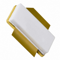
BLF6G10LS-135R,112 NXP Semiconductors, BLF6G10LS-135R,112 Datasheet - Page 55

BLF6G10LS-135R,112
Manufacturer Part Number
BLF6G10LS-135R,112
Description
IC BASESTATION FINAL SOT502B
Manufacturer
NXP Semiconductors
Datasheets
1.BLF6G20LS-140118.pdf
(100 pages)
2.BLF6G20LS-140112.pdf
(110 pages)
3.BLF6G10LS-135R112.pdf
(10 pages)
Specifications of BLF6G10LS-135R,112
Package / Case
SOT502B
Transistor Type
LDMOS
Frequency
871.5MHz
Gain
21dB
Voltage - Rated
65V
Current Rating
32A
Current - Test
950mA
Voltage - Test
28V
Power - Output
26.5W
Configuration
Single
Transistor Polarity
N-Channel
Resistance Drain-source Rds (on)
0.1 Ohms
Drain-source Breakdown Voltage
65 V
Gate-source Breakdown Voltage
13 V
Continuous Drain Current
32 A
Maximum Operating Temperature
+ 225 C
Mounting Style
SMD/SMT
Minimum Operating Temperature
- 65 C
Channel Type
N
Channel Mode
Enhancement
Drain Source Voltage (max)
65V
Output Power (max)
26.5W(Typ)
Power Gain (typ)@vds
21@28VdB
Frequency (min)
869MHz
Frequency (max)
894MHz
Package Type
LDMOST
Pin Count
3
Forward Transconductance (typ)
13S
Drain Source Resistance (max)
100(Typ)@6.15Vmohm
Reverse Capacitance (typ)
2@28VpF
Operating Temp Range
-65C to 225C
Drain Efficiency (typ)
28%
Mounting
Surface Mount
Mode Of Operation
2-Carrier W-CDMA
Number Of Elements
1
Vswr (max)
10
Screening Level
Military
Lead Free Status / RoHS Status
Lead free / RoHS Compliant
Noise Figure
-
Lead Free Status / Rohs Status
Compliant
Other names
934061247112
BLF6G10LS-135R
BLF6G10LS-135R
BLF6G10LS-135R
BLF6G10LS-135R
2.11
NXP QUBiC4 process technology
NXP's innovative high performance SiGe:C QUBiC4 process allows customers to incorporate
more functionality into devices with less space, competitive cost, superb reliability and significant
manufacturing advantages. Our state-of-the-art QUBiC4 technology and extensive IP availability
speeds the migration from GaAs components to silicon by enabling cutting-edge products with
best in class low-noise performance, linearity, power consumption, immunity to out-of-band signals,
spurious performance and output power. NXP’s QUBiC is a mature process in mass production
since 2002 with continuous performance upgrades since then. The QUBiC4 process is automotive
qualified and dual sourced in two high volume NXP-owned 8 inch waferfabs providing flexible, low
cost manufacturing with high yields and very low ppm in the field.
QUBiC4 in 3 variants, each having it’s benefits for specific
application areas:
QUBiC4+
The QUBiC4+ BiCMOS process features 0.25 μm CMOS with
5 metal layers for integration of dense digital logic based
smart functionality, a rich set of active and passive devices for
high-frequency mixed-signal designs including thick top metal
layers for high quality inductors. The device set; includinges a
37 GHz FT NPNs with 3.8 V breakdown voltage (BVce0) and
low noise figure (NF < 1.1 @ 2 GHz), 7 GHz fT VPNPs, a 28 GHz
high voltage NPN with 5.9 V breakdown voltage, differential
and single ended varicaps with Q-factor>30, scalable
inductors with Q-factor>20, 800 MHz FT lateral PNP’s,
0.25 μm CMOS, 137, 220 & 12 to 2000 ohm/sq. poly and
active resistors, a 270 ohm/sq. SiCr thin film resistor, a
5.7 fF/μm2 oxide capacitor and an 5 fF/μm2 MIM capacitor,
1 to 6 fF/μm2 oxide capacitors and various other devices
including L-PNPs, isolated NMOS, 3.3 V CMOS and RF-CMOS
transistorscapacitor. The QUBiC4+ process is: silicon based
and , ideal for applications up to 5 GHz (Ft = 37 GHz ,
NF < 1.1 dB @ 1.2 GHz) and e.g. for medium power amplifiers
up to 33 dBm.
QUBiC4X
The QUBiC4X BiCMOS process is a SiGe:C based extension
of the QUBiC process for high-frequency mixed signal designs
and offers on top of features the a rich set of devices for QUBiC
high-frequency mixed-signal designs; including also a 140 GHz
FT NPN with 2.5 V breakdown voltage and very low noise figure
(NF < 1.0 @ 10GHz). s, 0.25 μm CMOS, 220, a variety of resistors, a
5.7 fF/μm2 oxide capacitor and a 5 fF/μm2 MIM capacitor.
The QUBiC4X: first SiGe:C process is, ideal for applications
typically up to 30 GHz (Ft = 137 GHz , NF < 0.8dB @ 10 GHz)
and ultra low noise applications, e.g. LNAs and mixers.
Looking for the leader in SiGe:C? You've just found us!
QUBiC4Xi
The QUBiC4Xi BiCMOS process further enhances the QUBiC4X
process and offers additionally a features a set of devices for
high-frequency mixed-signal designs; including 180 GHz FT
NPNs with 1.4 V breakdown voltage and ultra-low noise figure
(NF < 0.7 @ 10 Ghz), 0.25 μm CMOS, several resistors,
a 5.7 fF/μm2 oxide capacitor and a 5 fF/μm2 MI capacitor.
QUBiC4Xi is the: newest SiGe:C process improved on Ft
(> 200 GHz) and even lower noise figure (NF < 0.5 7 dB @
10 GHz) and is, ideal for applications beyond 30 GHz, e.g.
LO generators.
NXP Semiconductors RF Manual 14
th
edition
57


