LPC47B272-MS SMSC, LPC47B272-MS Datasheet - Page 102
LPC47B272-MS
Manufacturer Part Number
LPC47B272-MS
Description
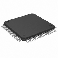
IC CTRLR SUPER I/O LPC 100-QFP
Manufacturer
SMSC
Datasheet
1.LPC47B272-MS.pdf
(195 pages)
Specifications of LPC47B272-MS
Controller Type
I/O Controller
Interface
LPC
Voltage - Supply
3.3V
Current - Supply
15mA
Operating Temperature
0°C ~ 70°C
Mounting Type
Surface Mount
Package / Case
100-QFP
Lead Free Status / RoHS Status
Lead free / RoHS Compliant
Other names
638-1019
Available stocks
Company
Part Number
Manufacturer
Quantity
Price
Company:

Part Number:
LPC47B272-MS
Manufacturer:
ADI
Quantity:
957
Company:
Part Number:
LPC47B272-MS
Manufacturer:
Microchip Technology
Quantity:
10 000
Part Number:
LPC47B272-MS
Manufacturer:
SMSC
Quantity:
20 000


IBF
OBF
EXTERNAL CLOCK SIGNAL
The LPC47B27x Keyboard Controller clock source is a 12 MHz clock generated from a 14.318 MHz clock.
The reset pulse must last for at least 24 16 MHz clock periods. The pulse-width requirement applies to
both internally (Vcc POR) and externally generated reset signals. In powerdown mode, the external clock
signal is not loaded by the chip.
DEFAULT RESET CONDITIONS
The LPC47B27x has one source of hardware reset: an external reset via the nPCI_RESET pin. Refer to
Table 46 for the effect of each type of reset on the internal registers.
GATEA20 AND KEYBOARD RESET
The LPC47B27x provides two options for GateA20 and Keyboard Reset: 8042 Software Generated
GateA20 and KRESET and Port 92 Fast GateA20 and KRESET.
PORT 92 FAST GATEA20 AND KEYBOARD RESET
Port 92 Register
This port can only be read or written if Port 92 has been enabled via bit 2 of the KRST_GA20
Register (Logical Device 7, 0xF0) set to 1.
This register is used to support the alternate reset (nALT_RST) and alternate A20 (ALT_A20) functions.
SMSC LPC47B27x
Bit
7:6
5
4
3
2
1
(Input Buffer Full)- This flag is set to 1 whenever the host system writes data into the input data
register. Setting this flag activates the LPC47B27x CPU's nIBF (MIRQ) interrupt if enabled.
When the LPC47B27x CPU reads the input data register (DBB), this bit is automatically reset and
the interrupt is cleared. There is no output pin associated with this internal signal.
(Output Buffer Full) - This flag is set to whenever the LPC47B27x CPU write to the output data
register (DBB). When the host system reads the output data register, this bit is automatically
reset.
Function
Reserved. Returns 00 when read
Reserved. Returns a 1 when read
Reserved. Returns a 0 when read
Reserved. Returns a 0 when read
Reserved. Returns a 1 when read
ALT_A20 Signal control. Writing a 0 to this bit causes the ALT_A20 signal to be
KCLK
KDAT
MCLK
MDAT
Host I/F Data Reg
Host I/F Status Reg
DESCRIPTION
Name
Location
Default Value
Attribute
Size
DATASHEET
N/A: Not Applicable
Table 54 - Resets
Port 92 Register
- 102 -
Port 92
92h
24h
Read/Write
8 bits
HARDWARE RESET
(nPCI_RESET)
Low
Low
Low
Low
00H
N/A
Rev. 04-17-07
Related parts for LPC47B272-MS
Image
Part Number
Description
Manufacturer
Datasheet
Request
R


Part Number:
Description:
FAST ETHERNET PHYSICAL LAYER DEVICE
Manufacturer:
SMSC Corporation
Datasheet:
Part Number:
Description:
357-036-542-201 CARDEDGE 36POS DL .156 BLK LOPRO
Manufacturer:
SMSC Corporation
Datasheet:
Part Number:
Description:
357-036-542-201 CARDEDGE 36POS DL .156 BLK LOPRO
Manufacturer:
SMSC Corporation
Datasheet:
Part Number:
Description:
357-036-542-201 CARDEDGE 36POS DL .156 BLK LOPRO
Manufacturer:
SMSC Corporation
Datasheet:
Part Number:
Description:
4-PORT USB2.0 HUB CONTROLLER
Manufacturer:
SMSC Corporation
Datasheet:
Part Number:
Description:
Manufacturer:
SMSC Corporation
Datasheet:
Part Number:
Description:
Manufacturer:
SMSC Corporation
Datasheet:
Part Number:
Description:
FDC37C672ENHANCED SUPER I/O CONTROLLER WITH FAST IR
Manufacturer:
SMSC Corporation
Datasheet:
Part Number:
Description:
COM90C66LJPARCNET Controller/Transceiver with AT Interface and On-Chip RAM
Manufacturer:
SMSC Corporation
Datasheet:
Part Number:
Description:
Manufacturer:
SMSC Corporation
Datasheet:
Part Number:
Description:
Manufacturer:
SMSC Corporation
Datasheet:
Part Number:
Description:
Manufacturer:
SMSC Corporation
Datasheet:
Part Number:
Description:
Manufacturer:
SMSC Corporation
Datasheet: