LPC47B272-MS SMSC, LPC47B272-MS Datasheet - Page 12
LPC47B272-MS
Manufacturer Part Number
LPC47B272-MS
Description
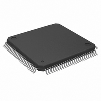
IC CTRLR SUPER I/O LPC 100-QFP
Manufacturer
SMSC
Datasheet
1.LPC47B272-MS.pdf
(195 pages)
Specifications of LPC47B272-MS
Controller Type
I/O Controller
Interface
LPC
Voltage - Supply
3.3V
Current - Supply
15mA
Operating Temperature
0°C ~ 70°C
Mounting Type
Surface Mount
Package / Case
100-QFP
Lead Free Status / RoHS Status
Lead free / RoHS Compliant
Other names
638-1019
Available stocks
Company
Part Number
Manufacturer
Quantity
Price
Company:

Part Number:
LPC47B272-MS
Manufacturer:
ADI
Quantity:
957
Company:
Part Number:
LPC47B272-MS
Manufacturer:
Microchip Technology
Quantity:
10 000
Part Number:
LPC47B272-MS
Manufacturer:
SMSC
Quantity:
20 000


Note 12: The TXD1 pin defaults to tristate following a VTR POR since the activate bit is ‘0’, which means Serial Port
Buffer Type Descriptions
Note: The buffer type values are specified at VCC=3.3V
IO12
IS/O12
O12
OD12
O6
O8
OD8
IO8
IS/O8
OD14
OP14
IOP14
IS/OP14
IOD16
O4
I
IS
PCI_IO
PCI_O
PCI_OD
PCI_I
PCI_ICLK
Note 1. See the PCI Local Bus Specification, Revision 2.1, Section 4.2.2.
Note 2. See the PCI Local Bus Specification, Revision 2.1, Section 4.2.2. and 4.2.3.
Pins That Require External Pullup Resistors
The following pins require external pullup resistors:
•
•
•
•
•
•
•
•
•
•
•
•
•
•
•
•
•
•
•
•
•
•
•
•
•
•
•
SMSC LPC47B27x
KDAT
KCLK
MDAT
MCLK
GP36/KBDRST if KBDRST function is used
GP37/A20M if A20M function is used
GP20/P17 If P17 function is used
GP21/P16 if P16 function is used
GP22/P12 if P12 function is used
GP27/nIO_SMI if nIO_SMI function is used as Open Drain Output
GP42/nIO_PME if nIO_PME function is used as Open Drain Output
SER_IRQ
GP40/DRVDEN0 if DRVDEN0 function is used as Open Drain
GP41/DRVDEN1 if DRVDEN1 function is used as Open Drain
nMTR0 if used as Open Drain Output
nDS0 if used as Open Drain Output
nDIR if used as Open Drain Output
nSTEP if used as Open Drain Output
nWDATA if used as Open Drain Output
nWGATE if used as Open Drain Output
nHDSEL if used as Open Drain Output
nINDEX
nTRK0
nWRTPRT
nRDATA
nDSKCHG
GP50-GP57 if the IRQx functions are used
1 is in the inactive state.
Input/Output, 12mA sink, 6mA source.
Input with Schmitt Trigger/Output, 12mA sink, 6mA source.
Output, 12mA sink, 6mA source.
Open Drain Output, 12mA sink.
Output, 6mA sink, 3mA source.
Output, 8mA sink, 4mA source.
Open Drain Output, 8mA sink.
Input/Output, 8mA sink, 4mA source.
Input with Schmitt Trigger/Output, 8mA sink, 4mA source.
Open Drain Output, 14mA sink.
Output, 14mA sink, 14mA source.
Input/Output, 14mA sink, 14mA source. Backdrive protected.
Input with Schmitt Trigger/Output, 14mA sink, 14mA source, Backdrive Protected.
Input/Output (Open Drain), 16mA sink.
Output, 4mA sink, 2mA source.
Input TTL Compatible.
Input with Schmitt Trigger.
Input/Output. These pins must meet the PCI 3.3V AC and DC Characteristics. (Note 1)
Output. These pins must meet the PCI 3.3V AC and DC Characteristics. (Note 1)
Open Drain Output. These pins must meet the PCI 3.3V AC and DC Characteristics.
(Note 1)
Input. These pins must meet the PCI 3.3V AC and DC Characteristics. (Note 1)
Clock Input. These pins must meet the PCI 3.3V AC and DC Characteristics and timing. (Note 2)
DATASHEET
- 12 -
Rev. 04-17-07
Related parts for LPC47B272-MS
Image
Part Number
Description
Manufacturer
Datasheet
Request
R


Part Number:
Description:
FAST ETHERNET PHYSICAL LAYER DEVICE
Manufacturer:
SMSC Corporation
Datasheet:
Part Number:
Description:
357-036-542-201 CARDEDGE 36POS DL .156 BLK LOPRO
Manufacturer:
SMSC Corporation
Datasheet:
Part Number:
Description:
357-036-542-201 CARDEDGE 36POS DL .156 BLK LOPRO
Manufacturer:
SMSC Corporation
Datasheet:
Part Number:
Description:
357-036-542-201 CARDEDGE 36POS DL .156 BLK LOPRO
Manufacturer:
SMSC Corporation
Datasheet:
Part Number:
Description:
4-PORT USB2.0 HUB CONTROLLER
Manufacturer:
SMSC Corporation
Datasheet:
Part Number:
Description:
Manufacturer:
SMSC Corporation
Datasheet:
Part Number:
Description:
Manufacturer:
SMSC Corporation
Datasheet:
Part Number:
Description:
FDC37C672ENHANCED SUPER I/O CONTROLLER WITH FAST IR
Manufacturer:
SMSC Corporation
Datasheet:
Part Number:
Description:
COM90C66LJPARCNET Controller/Transceiver with AT Interface and On-Chip RAM
Manufacturer:
SMSC Corporation
Datasheet:
Part Number:
Description:
Manufacturer:
SMSC Corporation
Datasheet:
Part Number:
Description:
Manufacturer:
SMSC Corporation
Datasheet:
Part Number:
Description:
Manufacturer:
SMSC Corporation
Datasheet:
Part Number:
Description:
Manufacturer:
SMSC Corporation
Datasheet: