MPC8379E-RDBA Freescale Semiconductor, MPC8379E-RDBA Datasheet - Page 110
MPC8379E-RDBA
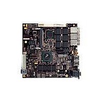
Manufacturer Part Number
MPC8379E-RDBA
Description
BOARD REF DESIGN MPC8379E
Manufacturer
Freescale Semiconductor
Series
PowerQUICC II™ PROr
Type
MPUr
Specifications of MPC8379E-RDBA
Contents
Board
Memory Type
Flash, SDRAM
Interface Type
Ethernet, USB, PCI, UART
Board Size
170 mm x 170 mm
Product
Modules
Silicon Manufacturer
Freescale
Core Architecture
Power Architecture
Core Sub-architecture
PowerQUICC
Silicon Core Number
MPC83xx
Silicon Family Name
PowerQUICC II PRO
Rohs Compliant
Yes
For Use With/related Products
MPC8379E
Lead Free Status / RoHS Status
Lead free / RoHS Compliant


System Design Information
These capacitors should have a value of 0.01 or 0.1 µF. Only ceramic SMT (surface mount technology)
capacitors should be used to minimize lead inductance, preferably 0402 or 0603 sizes.
In addition, it is recommended that there be several bulk storage capacitors distributed around the PCB,
feeding the VDD, OVDD, GVDD, and LVDD planes, to enable quick recharging of the smaller chip
capacitors. These bulk capacitors should have a low ESR (equivalent series resistance) rating to ensure the
quick response time necessary. They should also be connected to the power and ground planes through two
vias to minimize inductance. Suggested bulk capacitors—100–330 µF (AVX TPS tantalum or Sanyo
OSCON).
24.3
To ensure reliable operation, it is highly recommended that unused inputs be connected to an appropriate
signal level. Unused active low inputs should be tied to OVDD, GVDD, or LVDD as required. Unused
active high inputs should be connected to GND. All NC (no-connect) signals must remain unconnected.
Power and ground connections must be made to all external VDD, GVDD, LVDD, OVDD, and GND pins
of the device.
24.4
The device drivers are characterized over process, voltage, and temperature. For all buses, the driver is a
push-pull single-ended driver type (open drain for I
To measure Z
or GND. Then, the value of each resistor is varied until the pad voltage is OV
output impedance is the average of two components, the resistances of the pull-up and pull-down devices.
When data is held high, SW1 is closed (SW2 is open) and R
OV
other in value. Then, Z
110
DD
/2. R
Connection Recommendations
Output Buffer DC Impedance
P
then becomes the resistance of the pull-up devices. R
0
for the single-ended drivers, an external resistor is connected from the chip pad to OVDD
MPC8379E PowerQUICC II Pro Processor Hardware Specifications, Rev. 4
0
= (R
P
+ R
Figure 63. Driver Impedance Measurement
Data
N
)/2.
2
C).
Pad
P
R
R
is trimmed until the voltage at the pad equals
OVDD
OGND
N
P
P
and R
SW2
SW1
N
are designed to be close to each
DD
/2 (see
Freescale Semiconductor
Figure
63). The
Related parts for MPC8379E-RDBA
Image
Part Number
Description
Manufacturer
Datasheet
Request
R

Part Number:
Description:
BOARD REFERENCE FOR MPC837
Manufacturer:
Freescale Semiconductor
Datasheet:
Part Number:
Description:
BOARD PROCESSOR FOR MDS S
Manufacturer:
Freescale Semiconductor
Datasheet:

Part Number:
Description:
Powerquicc Ii Pro Processor Hardware Specifications
Manufacturer:
Freescale Semiconductor, Inc
Datasheet:

Part Number:
Description:
BOARD REF DES MPC8377 REV 2.1
Manufacturer:
Freescale Semiconductor
Datasheet:
Part Number:
Description:
Manufacturer:
Freescale Semiconductor, Inc
Datasheet:
Part Number:
Description:
Manufacturer:
Freescale Semiconductor, Inc
Datasheet:
Part Number:
Description:
Manufacturer:
Freescale Semiconductor, Inc
Datasheet:
Part Number:
Description:
Manufacturer:
Freescale Semiconductor, Inc
Datasheet:
Part Number:
Description:
Manufacturer:
Freescale Semiconductor, Inc
Datasheet:
Part Number:
Description:
Manufacturer:
Freescale Semiconductor, Inc
Datasheet:
Part Number:
Description:
Manufacturer:
Freescale Semiconductor, Inc
Datasheet:
Part Number:
Description:
Manufacturer:
Freescale Semiconductor, Inc
Datasheet:
Part Number:
Description:
Manufacturer:
Freescale Semiconductor, Inc
Datasheet:
Part Number:
Description:
Manufacturer:
Freescale Semiconductor, Inc
Datasheet:
Part Number:
Description:
Manufacturer:
Freescale Semiconductor, Inc
Datasheet: