MPC8379E-RDBA Freescale Semiconductor, MPC8379E-RDBA Datasheet - Page 45
MPC8379E-RDBA
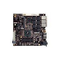
Manufacturer Part Number
MPC8379E-RDBA
Description
BOARD REF DESIGN MPC8379E
Manufacturer
Freescale Semiconductor
Series
PowerQUICC II™ PROr
Type
MPUr
Specifications of MPC8379E-RDBA
Contents
Board
Memory Type
Flash, SDRAM
Interface Type
Ethernet, USB, PCI, UART
Board Size
170 mm x 170 mm
Product
Modules
Silicon Manufacturer
Freescale
Core Architecture
Power Architecture
Core Sub-architecture
PowerQUICC
Silicon Core Number
MPC83xx
Silicon Family Name
PowerQUICC II PRO
Rohs Compliant
Yes
For Use With/related Products
MPC8379E
Lead Free Status / RoHS Status
Lead free / RoHS Compliant


Figure 26
Freescale Semiconductor
At recommended operating conditions OV
Input hold times: SD_CMD, SD_DATx, SD_CD to
SD_CLK
SD_CLK delay within device
Output valid: SD_CLK to SD_CMD, SD_DATx valid
Output hold: SD_CLK to SD_CMD, SD_DATx valid
SD card input setup
SD card input hold
SD card output valid
SD card output hold
Notes:
1
2
3
4
The symbols used for timing specifications herein follow the pattern of t
(reference)(state)
symbolizes eSDHC full mode speed device timing (SFS) input (I) to go invalid (X) with respect to the clock reference (K) going
to high (H). Also t
to the output (O) going valid (V) or data output valid time. Note that, in general, the clock reference symbol representation is
based on five letters representing the clock of a particular functional. For rise and fall times, the latter convention is used with
the appropriate letter: R (rise) or F (fall).
Measured at capacitive load of 40 pF.
For reference only, according to the SD card specifications.
Average, for reference only.
provides the eSDHC clock input timing diagram.
operational mode
External Clock
for inputs and t
Table 42. eSDHC AC Timing Specifications for Full-Speed Mode (continued)
SFSKHOV
eSDHC
Parameter
MPC8379E PowerQUICC II Pro Processor Hardware Specifications, Rev. 4
symbolizes eSDHC full speed timing (SFS) for the clock reference (K) to go high (H), with respect
(first three letters of functional block)(reference)(state)(signal)(state)
Figure 26. eSDHC Clock Input Timing Diagram
DD
VM
= 3.3 V ± 165 mV.
VM = Midpoint Voltage (OV
t
SFSCK
VM
t
INT_CLK_DLY
Symbol
t
t
t
SFSKHOV
SFSKHOX
SFSIXKH
t
ODLY
t
t
ISU
t
OH
IH
VM
1
(first three letters of functional block)(signal)(state)
DD
/2)
Enhanced Secure Digital Host Controller (eSDHC)
Min
t
1.5
—
—
SFSCKL
0
0
5
5
0
t
for outputs. For example, t
SFSCKR
Max
t
14
SFSCKH
—
—
—
—
—
—
4
t
SFSCKF
Unit
ns
ns
ns
ns
ns
ns
ns
—
SFSIXKH
Notes
—
2
4
2
3
3
3
3
45
Related parts for MPC8379E-RDBA
Image
Part Number
Description
Manufacturer
Datasheet
Request
R

Part Number:
Description:
BOARD REFERENCE FOR MPC837
Manufacturer:
Freescale Semiconductor
Datasheet:
Part Number:
Description:
BOARD PROCESSOR FOR MDS S
Manufacturer:
Freescale Semiconductor
Datasheet:

Part Number:
Description:
Powerquicc Ii Pro Processor Hardware Specifications
Manufacturer:
Freescale Semiconductor, Inc
Datasheet:

Part Number:
Description:
BOARD REF DES MPC8377 REV 2.1
Manufacturer:
Freescale Semiconductor
Datasheet:
Part Number:
Description:
Manufacturer:
Freescale Semiconductor, Inc
Datasheet:
Part Number:
Description:
Manufacturer:
Freescale Semiconductor, Inc
Datasheet:
Part Number:
Description:
Manufacturer:
Freescale Semiconductor, Inc
Datasheet:
Part Number:
Description:
Manufacturer:
Freescale Semiconductor, Inc
Datasheet:
Part Number:
Description:
Manufacturer:
Freescale Semiconductor, Inc
Datasheet:
Part Number:
Description:
Manufacturer:
Freescale Semiconductor, Inc
Datasheet:
Part Number:
Description:
Manufacturer:
Freescale Semiconductor, Inc
Datasheet:
Part Number:
Description:
Manufacturer:
Freescale Semiconductor, Inc
Datasheet:
Part Number:
Description:
Manufacturer:
Freescale Semiconductor, Inc
Datasheet:
Part Number:
Description:
Manufacturer:
Freescale Semiconductor, Inc
Datasheet:
Part Number:
Description:
Manufacturer:
Freescale Semiconductor, Inc
Datasheet: