MPC8379E-RDBA Freescale Semiconductor, MPC8379E-RDBA Datasheet - Page 75
MPC8379E-RDBA
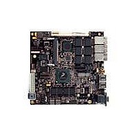
Manufacturer Part Number
MPC8379E-RDBA
Description
BOARD REF DESIGN MPC8379E
Manufacturer
Freescale Semiconductor
Series
PowerQUICC II™ PROr
Type
MPUr
Specifications of MPC8379E-RDBA
Contents
Board
Memory Type
Flash, SDRAM
Interface Type
Ethernet, USB, PCI, UART
Board Size
170 mm x 170 mm
Product
Modules
Silicon Manufacturer
Freescale
Core Architecture
Power Architecture
Core Sub-architecture
PowerQUICC
Silicon Core Number
MPC83xx
Silicon Family Name
PowerQUICC II PRO
Rohs Compliant
Yes
For Use With/related Products
MPC8379E
Lead Free Status / RoHS Status
Lead free / RoHS Compliant


Figure 53
assumes that the DC levels of the clock driver chip is compatible with device SerDes reference clock
input’s DC requirement.
Figure 54
Since LVDS clock driver’s common-mode voltage is higher than the device SerDes reference clock input’s
allowed range (100 to 400 mV), AC-coupled connection scheme must be used. It assumes the LVDS
Freescale Semiconductor
HCSL CLK Driver Chip
Total 50 Ω. Assume clock driver’s
output impedance is about 16 Ω.
Clock Driver
Clock Driver
Figure 53. DC-Coupled Differential Connection with HCSL Clock Driver (Reference Only)
shows the SerDes reference clock connection reference circuits for HCSL type clock driver. It
shows the SerDes reference clock connection reference circuits for LVDS type clock driver.
CLK_Out
CLK_Out
CLK_Out
Figure 53
fact that clock driver chip's internal structure, output impedance, and
termination requirements are different between various clock driver chip
manufacturers, it is very possible that the clock circuit reference designs
provided by the clock driver chip vendor are different from what is shown
below. They might also vary from one vendor to the other. Therefore,
Freescale Semiconductor can neither provide the optimal clock driver
reference circuits, nor guarantee the correctness of the following clock
driver connection reference circuits. The system designer is recommended
to contact the selected clock driver chip vendor for the optimal reference
circuits with the device SerDes reference clock receiver requirement
provided in this document.
MPC8379E PowerQUICC II Pro Processor Hardware Specifications, Rev. 4
to
33 Ω
33 Ω
Figure 56
Clock driver vendor dependent
source termination resistor
100 Ω differential PWB trace
below are for conceptual reference only. Due to the
NOTE
SDn_REF_CLK
SDn_REF_CLK
50 Ω
High-Speed Serial Interfaces (HSSI)
50 Ω
MPC8379E
SerDes Refer.
CLK Receiver
75
Related parts for MPC8379E-RDBA
Image
Part Number
Description
Manufacturer
Datasheet
Request
R

Part Number:
Description:
BOARD REFERENCE FOR MPC837
Manufacturer:
Freescale Semiconductor
Datasheet:
Part Number:
Description:
BOARD PROCESSOR FOR MDS S
Manufacturer:
Freescale Semiconductor
Datasheet:

Part Number:
Description:
Powerquicc Ii Pro Processor Hardware Specifications
Manufacturer:
Freescale Semiconductor, Inc
Datasheet:

Part Number:
Description:
BOARD REF DES MPC8377 REV 2.1
Manufacturer:
Freescale Semiconductor
Datasheet:
Part Number:
Description:
Manufacturer:
Freescale Semiconductor, Inc
Datasheet:
Part Number:
Description:
Manufacturer:
Freescale Semiconductor, Inc
Datasheet:
Part Number:
Description:
Manufacturer:
Freescale Semiconductor, Inc
Datasheet:
Part Number:
Description:
Manufacturer:
Freescale Semiconductor, Inc
Datasheet:
Part Number:
Description:
Manufacturer:
Freescale Semiconductor, Inc
Datasheet:
Part Number:
Description:
Manufacturer:
Freescale Semiconductor, Inc
Datasheet:
Part Number:
Description:
Manufacturer:
Freescale Semiconductor, Inc
Datasheet:
Part Number:
Description:
Manufacturer:
Freescale Semiconductor, Inc
Datasheet:
Part Number:
Description:
Manufacturer:
Freescale Semiconductor, Inc
Datasheet:
Part Number:
Description:
Manufacturer:
Freescale Semiconductor, Inc
Datasheet:
Part Number:
Description:
Manufacturer:
Freescale Semiconductor, Inc
Datasheet: