MPC8379E-RDBA Freescale Semiconductor, MPC8379E-RDBA Datasheet - Page 32
MPC8379E-RDBA
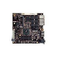
Manufacturer Part Number
MPC8379E-RDBA
Description
BOARD REF DESIGN MPC8379E
Manufacturer
Freescale Semiconductor
Series
PowerQUICC II™ PROr
Type
MPUr
Specifications of MPC8379E-RDBA
Contents
Board
Memory Type
Flash, SDRAM
Interface Type
Ethernet, USB, PCI, UART
Board Size
170 mm x 170 mm
Product
Modules
Silicon Manufacturer
Freescale
Core Architecture
Power Architecture
Core Sub-architecture
PowerQUICC
Silicon Core Number
MPC83xx
Silicon Family Name
PowerQUICC II PRO
Rohs Compliant
Yes
For Use With/related Products
MPC8379E
Lead Free Status / RoHS Status
Lead free / RoHS Compliant


USB
Figure 16
9
This section provides the AC and DC electrical characteristics for the USB dual-role controllers.
32
MDC rise time (20%–80%)
MDC fall time (80%–20%)
Note:
1
2
3
4
5
The symbols used for timing specifications herein follow the pattern of t
for inputs and t
management data timing (MD) for the time t
hold time. Also, t
latter convention is used with the appropriate letter: R (rise) or F (fall).
This parameter is dependent on the system clock speed. (The maximum frequency is the maximum platform frequency
divided by 64.)
This parameter is dependent on the system clock speed. (That is, for a system clock of 267 MHz, the maximum frequency
is 8.3 MHz and the minimum frequency is 1.2 MHz; for a system clock of 375 MHz, the maximum frequency is 11.7 MHz and
the minimum frequency is 1.7 MHz.)
Guaranteed by design.
t
valid state (V) relative to the t
plb_clk
USB
is the platform (CSB) clock divided according to the SCCR[TSEC1CM].
shows the MII management AC timing diagram.
Parameter
(first two letters of functional block)(reference)(state)(signal)(state)
MDDVKH
(Output)
(Input)
MDIO
MDIO
MDC
MPC8379E PowerQUICC II Pro Processor Hardware Specifications, Rev. 4
Table 33. MII Management AC Timing Specifications (continued)
symbolizes management data timing (MD) with respect to the time data input signals (D) reach the
Figure 16. MII Management Interface Timing Diagram
MDC
clock reference (K) going to the high (H) state or setup time. For rise and fall times, the
Symbol
t
MDCH
t
t
MDCR
MDCF
t
MDDVKH
MDC
t
1
MDC
t
MDKHDX
from clock reference (K) high (H) until data outputs (D) are invalid (X) or data
Min
—
—
t
MDCF
for outputs. For example, t
(first two letters of functional block)(signal)(state) (reference)(state)
Typical
t
MDDXKH
—
—
t
MDCR
Max
10
10
MDKHDX
Freescale Semiconductor
symbolizes
Unit
ns
ns
Notes
4
4
Related parts for MPC8379E-RDBA
Image
Part Number
Description
Manufacturer
Datasheet
Request
R

Part Number:
Description:
BOARD REFERENCE FOR MPC837
Manufacturer:
Freescale Semiconductor
Datasheet:
Part Number:
Description:
BOARD PROCESSOR FOR MDS S
Manufacturer:
Freescale Semiconductor
Datasheet:

Part Number:
Description:
Powerquicc Ii Pro Processor Hardware Specifications
Manufacturer:
Freescale Semiconductor, Inc
Datasheet:

Part Number:
Description:
BOARD REF DES MPC8377 REV 2.1
Manufacturer:
Freescale Semiconductor
Datasheet:
Part Number:
Description:
Manufacturer:
Freescale Semiconductor, Inc
Datasheet:
Part Number:
Description:
Manufacturer:
Freescale Semiconductor, Inc
Datasheet:
Part Number:
Description:
Manufacturer:
Freescale Semiconductor, Inc
Datasheet:
Part Number:
Description:
Manufacturer:
Freescale Semiconductor, Inc
Datasheet:
Part Number:
Description:
Manufacturer:
Freescale Semiconductor, Inc
Datasheet:
Part Number:
Description:
Manufacturer:
Freescale Semiconductor, Inc
Datasheet:
Part Number:
Description:
Manufacturer:
Freescale Semiconductor, Inc
Datasheet:
Part Number:
Description:
Manufacturer:
Freescale Semiconductor, Inc
Datasheet:
Part Number:
Description:
Manufacturer:
Freescale Semiconductor, Inc
Datasheet:
Part Number:
Description:
Manufacturer:
Freescale Semiconductor, Inc
Datasheet:
Part Number:
Description:
Manufacturer:
Freescale Semiconductor, Inc
Datasheet: