DK-DEV-1AGX60N Altera, DK-DEV-1AGX60N Datasheet - Page 10
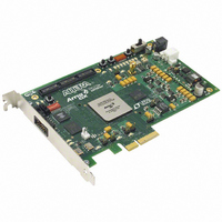
DK-DEV-1AGX60N
Manufacturer Part Number
DK-DEV-1AGX60N
Description
KIT DEV ARRIA GX 1AGX60N
Manufacturer
Altera
Series
Arria GXr
Type
FPGAr
Datasheet
1.EP1AGX20CF484C6N.pdf
(234 pages)
Specifications of DK-DEV-1AGX60N
Contents
Dev. Board, Quartus® II Web Edition, Reference Designs, Labs, and Complete Documentation
For Use With/related Products
1AGX60N
Lead Free Status / RoHS Status
Lead free / RoHS Compliant
Other names
544-2372
Available stocks
Company
Part Number
Manufacturer
Quantity
Price


2–4
Figure 2–3. Clock Multiplier Unit
Figure 2–4. Transmitter PLL
Notes to
(1) You only need to select the protocol and the available input reference clock frequency in the ALTGXB MegaWizard Plug-In Manager. Based on your
(2) The global clock line must be driven from an input pin only.
Arria GX Device Handbook, Volume 1
Inter-Transceiver Lines
selections, the MegaWizard Plug-In Manager automatically selects the necessary /M and /L dividers (clock multiplication factors).
Global Clock
Dedicated
REFCLK0
Dedicated
REFCLK1
Inter-Transceiver Lines[2:0]
Figure
To
2–4:
(2)
CMU Block
Reference Clock
Global Clock (1),
Inter-Transceiver
Figure 2–3
The transmitter PLL multiplies the input reference clock to generate the high-speed
serial clock required to support the intended protocol. It implements a half-rate
voltage controlled oscillator (VCO) that generates a clock at half the frequency of the
serial data rate for which it is configured.
Figure 2–4
/2
/2
The reference clock input to the transmitter PLL can be derived from:
■
■
from REFCLKs,
Lines
One of two available dedicated reference clock input pins (REFCLK0 or REFCLK1)
of the associated transceiver block
PLD global clock network (must be driven directly from an input clock pin and
cannot be driven by user logic or enhanced PLL)
shows the block diagram of the clock multiplier unit.
shows the block diagram of the transmitter PLL.
Transmitter Channels [3:2]
Transmitter Channels [1:0]
INCLK
Transmitter
PLL
Frequency
Detector
Phase
down
up
/M
(1)
Pump + Loop
Central Clock
Gen Block
Divider Block
Divider Block
Gen Block
Local Clock
Local Clock
Charge
TX Clock
TX Clock
Filter
Divider
Block
Controlled
Oscillator
Voltage
Transmitter PLL
and Low-Speed Parallel Clocks
and Low-Speed Parallel Clocks
Transmitter High-Speed Serial
Transmitter High-Speed Serial
© December 2009 Altera Corporation
Chapter 2: Arria GX Architecture
/L
(1)
Serial Clock
High Speed
Transceivers
Related parts for DK-DEV-1AGX60N
Image
Part Number
Description
Manufacturer
Datasheet
Request
R

Part Number:
Description:
KIT DEV ARRIA II GX FPGA 2AGX125
Manufacturer:
Altera
Datasheet:

Part Number:
Description:
KIT DEV CYCLONE III LS EP3CLS200
Manufacturer:
Altera
Datasheet:

Part Number:
Description:
KIT DEV STRATIX IV FPGA 4SE530
Manufacturer:
Altera
Datasheet:

Part Number:
Description:
KIT DEV FPGA 2AGX260 W/6.375G TX
Manufacturer:
Altera
Datasheet:

Part Number:
Description:
KIT DEV MAX V 5M570Z
Manufacturer:
Altera
Datasheet:

Part Number:
Description:
KIT DEV STRATIX V FPGA 5SGXEA7
Manufacturer:
Altera
Datasheet:

Part Number:
Description:
KIT DEVELOPMENT STRATIX III
Manufacturer:
Altera
Datasheet:

Part Number:
Description:
KIT DEVELOPMENT STRATIX IV
Manufacturer:
Altera
Datasheet:
Part Number:
Description:
KIT STARTER CYCLONE IV GX
Manufacturer:
Altera
Datasheet:
Part Number:
Description:
KIT DEVELOPMENT STRATIX IV
Manufacturer:
Altera
Datasheet:

Part Number:
Description:
CPLD, EP610 Family, ECMOS Process, 300 Gates, 16 Macro Cells, 16 Reg., 16 User I/Os, 5V Supply, 35 Speed Grade, 24DIP
Manufacturer:
Altera Corporation
Datasheet:
Part Number:
Description:
CPLD, EP610 Family, ECMOS Process, 300 Gates, 16 Macro Cells, 16 Reg., 16 User I/Os, 5V Supply, 15 Speed Grade, 24DIP
Manufacturer:
Altera Corporation
Datasheet: