DK-DEV-1AGX60N Altera, DK-DEV-1AGX60N Datasheet - Page 124
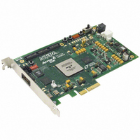
DK-DEV-1AGX60N
Manufacturer Part Number
DK-DEV-1AGX60N
Description
KIT DEV ARRIA GX 1AGX60N
Manufacturer
Altera
Series
Arria GXr
Type
FPGAr
Datasheet
1.EP1AGX20CF484C6N.pdf
(234 pages)
Specifications of DK-DEV-1AGX60N
Contents
Dev. Board, Quartus® II Web Edition, Reference Designs, Labs, and Complete Documentation
For Use With/related Products
1AGX60N
Lead Free Status / RoHS Status
Lead free / RoHS Compliant
Other names
544-2372
Available stocks
Company
Part Number
Manufacturer
Quantity
Price


4–2
Table 4–1. Arria GX Device Absolute Maximum Ratings
Recommended Operating Conditions
Table 4–3. Arria GX Device Recommended Operating Conditions (Part 1 of 2)
Arria GX Device Handbook, Volume 1
T
Notes to
(1) For more information about operating requirements for Altera
(2) Conditions beyond those listed in
(3) Supply voltage specifications apply to voltage readings taken at the device pins, not at the power supply.
(4) During transitions, the inputs may overshoot to the voltage shown in
V
V
V
V
V
J
CCINT
CCIO
CCPD
I
O
Symbol
ratings for extended periods of time may have adverse affects on the device.
100% duty cycle. During transitions, the inputs may undershoot to –2.0 V for input currents less than 100 mA and periods shorter than 20 ns.
Symbol
Table
4–1:
Supply voltage for internal
logic and input buffers
Supply voltage for output
buffers, 3.3-V operation
Supply voltage for output
buffers, 2.5-V operation
Supply voltage for output
buffers, 1.8-V operation
Supply voltage for output
buffers, 1.5-V operation
Supply voltage for output
buffers, 1.2-V operation
Supply voltage for pre-drivers
as well as configuration and
JTAG I/O buffers.
Input voltage
(refer to
Output voltage
Junction temperature
Table 4–2. Maximum Duty Cycles in Voltage Transitions
Table 4–3
Note to
(1) During transition, the inputs may overshoot to the voltages shown based on the input duty cycle. The DC case is
Table
Parameter
equivalent to 100% duty cycle.
Parameter
Symbol
Table
4–2)
Table 4–1
V
I
lists the recommended operating conditions for the Arria GX device family.
4–2:
may cause permanent damage to a device. Additionally, device operation at the absolute maximum
Maximum duty cycles in
voltage transitions
BGA packages under bias
Rise time 100 ms
Rise time 100 ms (3),
Rise time 100 ms
Rise time 100 ms
Rise time 100 ms
Rise time 100 ms
100 s rise time 100 ms
(2),
Parameter
(5)
®
devices, refer to the
Conditions
(Note
Table 4–2
Conditions
—
1), (2),
based upon the input duty cycle. The DC case is equivalent to
(3)
(3)
(3)
(3)
(3)
Arria GX Device Family Data Sheet
(6)
(3)
Condition
V
V
V
V
V
V
I
I
I
I
I
I
= 4.0 V
= 4.2 V
= 4.3 V
= 4.4 V
= 4.5 V
= 4.1 V
(Part 2 of 2)
(4)
Minimum
(Note 1)
–55
Chapter 4: DC and Switching Characteristics
(Note 1)
Minimum
(3.00)
3.135
2.375
1.425
3.135
© December 2009 Altera Corporation
1.15
1.71
1.15
–0.5
0
(Part 1 of 2)
Maximum Duty Cycles (%)
Maximum
125
Maximum
(3.60)
chapter.
3.465
2.625
1.575
3.465
V
100
1.25
1.89
1.25
4.0
Operating Conditions
90
50
30
17
10
CCIO
Units
C
Units
V
V
V
V
V
V
V
V
V
Related parts for DK-DEV-1AGX60N
Image
Part Number
Description
Manufacturer
Datasheet
Request
R

Part Number:
Description:
KIT DEV ARRIA II GX FPGA 2AGX125
Manufacturer:
Altera
Datasheet:

Part Number:
Description:
KIT DEV CYCLONE III LS EP3CLS200
Manufacturer:
Altera
Datasheet:

Part Number:
Description:
KIT DEV STRATIX IV FPGA 4SE530
Manufacturer:
Altera
Datasheet:

Part Number:
Description:
KIT DEV FPGA 2AGX260 W/6.375G TX
Manufacturer:
Altera
Datasheet:

Part Number:
Description:
KIT DEV MAX V 5M570Z
Manufacturer:
Altera
Datasheet:

Part Number:
Description:
KIT DEV STRATIX V FPGA 5SGXEA7
Manufacturer:
Altera
Datasheet:

Part Number:
Description:
KIT DEVELOPMENT STRATIX III
Manufacturer:
Altera
Datasheet:

Part Number:
Description:
KIT DEVELOPMENT STRATIX IV
Manufacturer:
Altera
Datasheet:
Part Number:
Description:
KIT STARTER CYCLONE IV GX
Manufacturer:
Altera
Datasheet:
Part Number:
Description:
KIT DEVELOPMENT STRATIX IV
Manufacturer:
Altera
Datasheet:

Part Number:
Description:
CPLD, EP610 Family, ECMOS Process, 300 Gates, 16 Macro Cells, 16 Reg., 16 User I/Os, 5V Supply, 35 Speed Grade, 24DIP
Manufacturer:
Altera Corporation
Datasheet:
Part Number:
Description:
CPLD, EP610 Family, ECMOS Process, 300 Gates, 16 Macro Cells, 16 Reg., 16 User I/Os, 5V Supply, 15 Speed Grade, 24DIP
Manufacturer:
Altera Corporation
Datasheet: