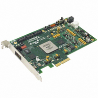
DK-DEV-1AGX60N Altera, DK-DEV-1AGX60N Datasheet - Page 18

DK-DEV-1AGX60N
Manufacturer Part Number
DK-DEV-1AGX60N
Description
KIT DEV ARRIA GX 1AGX60N
Manufacturer
Altera
Series
Arria GXr
Type
FPGAr
Datasheet
1.EP1AGX20CF484C6N.pdf
(234 pages)
Specifications of DK-DEV-1AGX60N
Contents
Dev. Board, Quartus® II Web Edition, Reference Designs, Labs, and Complete Documentation
For Use With/related Products
1AGX60N
Lead Free Status / RoHS Status
Lead free / RoHS Compliant
Other names
544-2372
Available stocks
Company
Part Number
Manufacturer
Quantity
Price
- Current page: 18 of 234
- Download datasheet (4Mb)
2–12
Figure 2–13. Receiver PLL and Clock Recovery Unit
Notes to
(1) You only need to select the protocol and the available input reference clock frequency in the ALTGXB MegaWizard Plug-In Manager. Based on your
(2) The global clock line must be driven from an input pin only.
Arria GX Device Handbook, Volume 1
Dedicated
REFCLK1
Inter-Transceiver Lines
Global Clock (2)
REFCLK0
Dedicated
selections, the ALTGXB MegaWizard Plug-In Manager automatically selects the necessary /M and /L dividers.
Figure
2–13:
[2:0]
rx_locktorefclk
/2
/2
rx_locktodata
rx_datain
The receiver equalization circuit is comprised of a programmable amplifier. Each
stage is a peaking equalizer with a different center frequency and programmable gain.
This allows varying amounts of gain to be applied, depending on the overall
frequency response of the channel loss. Channel loss is defined as the summation of
all losses through the PCB traces, vias, connectors, and cables present in the physical
link. The Quartus II software allows five equalization settings for Arria GX devices.
Receiver PLL and Clock Recovery Unit (CRU)
Each transceiver block has four receiver PLLs and CRU units, each of which is
dedicated to a receiver channel. The receiver PLL is fed by an input reference clock.
The receiver PLL, in conjunction with the CRU, generates two clocks: a high-speed
serial recovered clock that clocks the deserializer and a low-speed parallel recovered
clock that clocks the receiver's digital logic.
Figure 2–13
The reference clock input to the receiver PLL can be derived from:
■
■
■
All the parameters listed are programmable in the Quartus II software. The receiver
PLL has the following features:
■
■
■
■
One of the two available dedicated reference clock input pins (REFCLK0 or
REFCLK1) of the associated transceiver block
PLD global clock network (must be driven directly from an input clock pin and
cannot be driven by user logic or enhanced PLL)
Inter-transceiver block lines driven by reference clock input pins of other
transceiver blocks
Operates from 600 Mbps to 3.125 Gbps.
Uses a reference clock between 50 MHz and 622.08 MHz.
Programmable bandwidth settings: low, medium, and high.
Programmable rx_locktorefclk (forces the receiver PLL to lock to reference
clock) and rx_locktodata (forces the receiver PLL to lock to data).
shows a block diagram of the receiver PLL and CRU circuits.
rx_cruclk
Clock Recovery Unit ( CRU ) Control
PFD
up
dn
/M
up
dn
rx_pll_locked
CP+ LF
© December 2009 Altera Corporation
VCO
Chapter 2: Arria GX Architecture
High-speed serial recovered clk
Low-speed parallel recovered clk
rx_freqlocked
/L
Transceivers
Related parts for DK-DEV-1AGX60N
Image
Part Number
Description
Manufacturer
Datasheet
Request
R

Part Number:
Description:
KIT DEV ARRIA II GX FPGA 2AGX125
Manufacturer:
Altera
Datasheet:

Part Number:
Description:
KIT DEV CYCLONE III LS EP3CLS200
Manufacturer:
Altera
Datasheet:

Part Number:
Description:
KIT DEV STRATIX IV FPGA 4SE530
Manufacturer:
Altera
Datasheet:

Part Number:
Description:
KIT DEV FPGA 2AGX260 W/6.375G TX
Manufacturer:
Altera
Datasheet:

Part Number:
Description:
KIT DEV MAX V 5M570Z
Manufacturer:
Altera
Datasheet:

Part Number:
Description:
KIT DEV STRATIX V FPGA 5SGXEA7
Manufacturer:
Altera
Datasheet:

Part Number:
Description:
KIT DEVELOPMENT STRATIX III
Manufacturer:
Altera
Datasheet:

Part Number:
Description:
KIT DEVELOPMENT STRATIX IV
Manufacturer:
Altera
Datasheet:

Part Number:
Description:
KIT STARTER CYCLONE IV GX
Manufacturer:
Altera
Datasheet:

Part Number:
Description:
KIT DEVELOPMENT STRATIX IV
Manufacturer:
Altera
Datasheet:

Part Number:
Description:
CPLD, EP610 Family, ECMOS Process, 300 Gates, 16 Macro Cells, 16 Reg., 16 User I/Os, 5V Supply, 35 Speed Grade, 24DIP
Manufacturer:
Altera Corporation
Datasheet:

Part Number:
Description:
CPLD, EP610 Family, ECMOS Process, 300 Gates, 16 Macro Cells, 16 Reg., 16 User I/Os, 5V Supply, 15 Speed Grade, 24DIP
Manufacturer:
Altera Corporation
Datasheet:


