DK-DEV-1AGX60N Altera, DK-DEV-1AGX60N Datasheet - Page 55
DK-DEV-1AGX60N
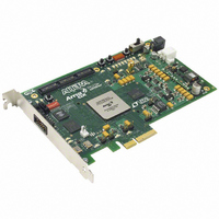
Manufacturer Part Number
DK-DEV-1AGX60N
Description
KIT DEV ARRIA GX 1AGX60N
Manufacturer
Altera
Series
Arria GXr
Type
FPGAr
Datasheet
1.EP1AGX20CF484C6N.pdf
(234 pages)
Specifications of DK-DEV-1AGX60N
Contents
Dev. Board, Quartus® II Web Edition, Reference Designs, Labs, and Complete Documentation
For Use With/related Products
1AGX60N
Lead Free Status / RoHS Status
Lead free / RoHS Compliant
Other names
544-2372
Available stocks
Company
Part Number
Manufacturer
Quantity
Price


Chapter 2: Arria GX Architecture
TriMatrix Memory
Table 2–11. TriMatrix Memory Features (Part 2 of 2)
M512 RAM Block
© December 2009 Altera Corporation
ROM
FIFO buffer
Pack mode
Byte enable
Address clock enable
Parity bits
Mixed clock mode
Memory initialization file (.mif)
Simple dual-port memory mixed width support
True dual-port memory mixed width support
Power-up conditions
Register clears
Mixed-port read-during-write
Configurations
Memory Feature
TriMatrix memory provides three different memory sizes for efficient application
support. The Quartus II software automatically partitions the user-defined memory
into the embedded memory blocks using the most efficient size combinations. You can
also manually assign the memory to a specific block size or a mixture of block sizes.
The M512 RAM block is a simple dual-port memory block and is useful for
implementing small FIFO buffers, DSP, and clock domain transfer applications. Each
block contains 576 RAM bits (including parity bits). M512 RAM blocks can be
configured in the following modes:
■
■
■
■
■
Simple dual-port RAM
Single-port RAM
FIFO
ROM
Shift register
Unknown output/old
M512 RAM Block
Output registers
Outputs cleared
(32 × 18 Bits)
512 × 1
256 × 2
128 × 4
32 × 16
32 × 18
64 × 8
64 × 9
data
v
v
—
v
—
v
v
v
v
—
Unknown output/old
M4K RAM Block
Output registers
Outputs cleared
(128 × 36 Bits)
256 × 16
256 × 18
128 × 32
128 × 36
512 × 8
512 × 9
4K × 1
2K × 2
1K × 4
data
v
v
v
v
v
v
v
v
v
v
Arria GX Device Handbook, Volume 1
Outputs unknown
Unknown output
Output registers
(4K × 144 Bits)
M-RAM Block
32K × 16
32K × 18
16K × 32
16K × 36
4K × 128
4K × 144
64K × 8
64K × 9
8K × 64
8K × 72
v
v
v
v
v
v
v
v
—
—
2–49
Related parts for DK-DEV-1AGX60N
Image
Part Number
Description
Manufacturer
Datasheet
Request
R

Part Number:
Description:
KIT DEV ARRIA II GX FPGA 2AGX125
Manufacturer:
Altera
Datasheet:

Part Number:
Description:
KIT DEV CYCLONE III LS EP3CLS200
Manufacturer:
Altera
Datasheet:

Part Number:
Description:
KIT DEV STRATIX IV FPGA 4SE530
Manufacturer:
Altera
Datasheet:

Part Number:
Description:
KIT DEV FPGA 2AGX260 W/6.375G TX
Manufacturer:
Altera
Datasheet:

Part Number:
Description:
KIT DEV MAX V 5M570Z
Manufacturer:
Altera
Datasheet:

Part Number:
Description:
KIT DEV STRATIX V FPGA 5SGXEA7
Manufacturer:
Altera
Datasheet:

Part Number:
Description:
KIT DEVELOPMENT STRATIX III
Manufacturer:
Altera
Datasheet:

Part Number:
Description:
KIT DEVELOPMENT STRATIX IV
Manufacturer:
Altera
Datasheet:
Part Number:
Description:
KIT STARTER CYCLONE IV GX
Manufacturer:
Altera
Datasheet:
Part Number:
Description:
KIT DEVELOPMENT STRATIX IV
Manufacturer:
Altera
Datasheet:

Part Number:
Description:
CPLD, EP610 Family, ECMOS Process, 300 Gates, 16 Macro Cells, 16 Reg., 16 User I/Os, 5V Supply, 35 Speed Grade, 24DIP
Manufacturer:
Altera Corporation
Datasheet:
Part Number:
Description:
CPLD, EP610 Family, ECMOS Process, 300 Gates, 16 Macro Cells, 16 Reg., 16 User I/Os, 5V Supply, 15 Speed Grade, 24DIP
Manufacturer:
Altera Corporation
Datasheet: