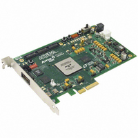
DK-DEV-1AGX60N Altera, DK-DEV-1AGX60N Datasheet - Page 27

DK-DEV-1AGX60N
Manufacturer Part Number
DK-DEV-1AGX60N
Description
KIT DEV ARRIA GX 1AGX60N
Manufacturer
Altera
Series
Arria GXr
Type
FPGAr
Datasheet
1.EP1AGX20CF484C6N.pdf
(234 pages)
Specifications of DK-DEV-1AGX60N
Contents
Dev. Board, Quartus® II Web Edition, Reference Designs, Labs, and Complete Documentation
For Use With/related Products
1AGX60N
Lead Free Status / RoHS Status
Lead free / RoHS Compliant
Other names
544-2372
Available stocks
Company
Part Number
Manufacturer
Quantity
Price
- Current page: 27 of 234
- Download datasheet (4Mb)
Chapter 2: Arria GX Architecture
Transceivers
Figure 2–19. Arria GX Block in Reverse Serial Loopback Mode
© December 2009 Altera Corporation
FPGA
Logic
Array
Transmitter Digital Logic
Receiver Digital Logic
Incremental
Incremental
Generator
RX Phase
Compen-
Verify
BIST
BIST
sation
FIFO
Compensation
TX Phase
1
FIFO
In GIGE and Serial RapidIO modes, you can dynamically put each transceiver
channel individually in serial loopback by controlling the rx_seriallpbken port. A
high on the rx_seriallpbken port puts the transceiver into serial loopback and a
low takes the transceiver out of serial loopback.
As seen in
back to the receiver CRU in serial loopback. The transmitter data path from the PLD
interface to the serializer in serial loopback is the same as in non-loopback mode. The
receiver data path from the clock recovery unit to the PLD interface in serial loopback
is the same as in non-loopback mode. Because the entire transceiver data path is
available in serial loopback, this option is often used to diagnose the data path as a
probable cause of link errors.
When serial loopback is enabled, the transmitter output buffer is still active and
drives the serial data out on the tx_dataout port.
Reverse Serial Loopback
Reverse serial loopback mode uses the analog portion of the transceiver. An external
source (pattern generator or transceiver) generates the source data. The high-speed
serial source data arrives at the high-speed differential receiver input buffer, passes
through the CRU unit and the retimed serial data is looped back, and is transmitted
though the high-speed differential transmitter output buffer.
Figure 2–19
Serializer
Byte
Figure
shows the data path in reverse serial loopback mode.
20
serializer
Byte
De-
Encoder
8B/10B
2–18, the serial data output from the transmitter serializer is looped
Decoder
8B/10B
Generator
PRBS
BIST
Match
Rate
FIFO
Deskew
FIFO
PRBS
Verify
BIST
Aligner
Word
Arria GX Device Handbook, Volume 1
Analog Receiver and
Transmitter Logic
Serializer
serializer
De-
Reverse
Serial
Loopback
Recovery
Clock
Unit
2–21
Related parts for DK-DEV-1AGX60N
Image
Part Number
Description
Manufacturer
Datasheet
Request
R

Part Number:
Description:
KIT DEV ARRIA II GX FPGA 2AGX125
Manufacturer:
Altera
Datasheet:

Part Number:
Description:
KIT DEV CYCLONE III LS EP3CLS200
Manufacturer:
Altera
Datasheet:

Part Number:
Description:
KIT DEV STRATIX IV FPGA 4SE530
Manufacturer:
Altera
Datasheet:

Part Number:
Description:
KIT DEV FPGA 2AGX260 W/6.375G TX
Manufacturer:
Altera
Datasheet:

Part Number:
Description:
KIT DEV MAX V 5M570Z
Manufacturer:
Altera
Datasheet:

Part Number:
Description:
KIT DEV STRATIX V FPGA 5SGXEA7
Manufacturer:
Altera
Datasheet:

Part Number:
Description:
KIT DEVELOPMENT STRATIX III
Manufacturer:
Altera
Datasheet:

Part Number:
Description:
KIT DEVELOPMENT STRATIX IV
Manufacturer:
Altera
Datasheet:

Part Number:
Description:
KIT STARTER CYCLONE IV GX
Manufacturer:
Altera
Datasheet:

Part Number:
Description:
KIT DEVELOPMENT STRATIX IV
Manufacturer:
Altera
Datasheet:

Part Number:
Description:
CPLD, EP610 Family, ECMOS Process, 300 Gates, 16 Macro Cells, 16 Reg., 16 User I/Os, 5V Supply, 35 Speed Grade, 24DIP
Manufacturer:
Altera Corporation
Datasheet:

Part Number:
Description:
CPLD, EP610 Family, ECMOS Process, 300 Gates, 16 Macro Cells, 16 Reg., 16 User I/Os, 5V Supply, 15 Speed Grade, 24DIP
Manufacturer:
Altera Corporation
Datasheet:


