DK-DEV-1AGX60N Altera, DK-DEV-1AGX60N Datasheet - Page 95
DK-DEV-1AGX60N
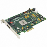
Manufacturer Part Number
DK-DEV-1AGX60N
Description
KIT DEV ARRIA GX 1AGX60N
Manufacturer
Altera
Series
Arria GXr
Type
FPGAr
Datasheet
1.EP1AGX20CF484C6N.pdf
(234 pages)
Specifications of DK-DEV-1AGX60N
Contents
Dev. Board, Quartus® II Web Edition, Reference Designs, Labs, and Complete Documentation
For Use With/related Products
1AGX60N
Lead Free Status / RoHS Status
Lead free / RoHS Compliant
Other names
544-2372
Available stocks
Company
Part Number
Manufacturer
Quantity
Price


Chapter 2: Arria GX Architecture
I/O Structure
Figure 2–75. Arria GX IOE in DDR Output I/O Configuration
Notes to
(1) All input signals to the IOE can be inverted at the IOE.
(2) The tri-state buffer is active low. The DDIO megafunction represents the tri-state buffer as active-high with an inverter at the OE register data port.
(3) The optional PCI clamp is only available on column I/O pins.
© December 2009 Altera Corporation
Figure
Column, Row,
Interconnect
or Local
2–75:
ioe_clk[7..0]
When using the IOE for DDR outputs, the two output registers are configured to clock
two data paths from ALMs on rising clock edges. These output registers are
multiplexed by the clock to drive the output pin at a ×2 rate. One output register
clocks the first bit out on the clock high time, while the other output register clocks the
second bit out on the clock low time.
output.
clkout
aclr/apreset
sclr/spreset
ce_out
oe
Figure 2–76
Chip-Wide Reset
shows the DDR output timing diagram.
Output Register
Output Register
OE Register
OE Register
ENA
Notes (1), (2)
CLRN/PRN
CLRN/PRN
CLRN/PRN
CLRN/PRN
D
ENA
D
ENA
D
ENA
D
Q
Q
Q
Q
Figure 2–75
Used for
DDR, DDR2
SDRAM
clk
Open-Drain Output
Drive Strength
Pin Delay
Output
Control
shows the IOE configured for DDR
OE Register
t CO Delay
V CCIO
Arria GX Device Handbook, Volume 1
V CCIO
PCI Clamp (3)
Termination
On-Chip
Bus-Hold
Circuit
Programmable
Pull-Up
Resistor
2–89
Related parts for DK-DEV-1AGX60N
Image
Part Number
Description
Manufacturer
Datasheet
Request
R

Part Number:
Description:
KIT DEV ARRIA II GX FPGA 2AGX125
Manufacturer:
Altera
Datasheet:

Part Number:
Description:
KIT DEV CYCLONE III LS EP3CLS200
Manufacturer:
Altera
Datasheet:

Part Number:
Description:
KIT DEV STRATIX IV FPGA 4SE530
Manufacturer:
Altera
Datasheet:

Part Number:
Description:
KIT DEV FPGA 2AGX260 W/6.375G TX
Manufacturer:
Altera
Datasheet:

Part Number:
Description:
KIT DEV MAX V 5M570Z
Manufacturer:
Altera
Datasheet:

Part Number:
Description:
KIT DEV STRATIX V FPGA 5SGXEA7
Manufacturer:
Altera
Datasheet:

Part Number:
Description:
KIT DEVELOPMENT STRATIX III
Manufacturer:
Altera
Datasheet:

Part Number:
Description:
KIT DEVELOPMENT STRATIX IV
Manufacturer:
Altera
Datasheet:
Part Number:
Description:
KIT STARTER CYCLONE IV GX
Manufacturer:
Altera
Datasheet:
Part Number:
Description:
KIT DEVELOPMENT STRATIX IV
Manufacturer:
Altera
Datasheet:

Part Number:
Description:
CPLD, EP610 Family, ECMOS Process, 300 Gates, 16 Macro Cells, 16 Reg., 16 User I/Os, 5V Supply, 35 Speed Grade, 24DIP
Manufacturer:
Altera Corporation
Datasheet:
Part Number:
Description:
CPLD, EP610 Family, ECMOS Process, 300 Gates, 16 Macro Cells, 16 Reg., 16 User I/Os, 5V Supply, 15 Speed Grade, 24DIP
Manufacturer:
Altera Corporation
Datasheet: