DK-DEV-1AGX60N Altera, DK-DEV-1AGX60N Datasheet - Page 154
DK-DEV-1AGX60N
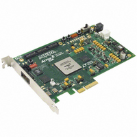
Manufacturer Part Number
DK-DEV-1AGX60N
Description
KIT DEV ARRIA GX 1AGX60N
Manufacturer
Altera
Series
Arria GXr
Type
FPGAr
Datasheet
1.EP1AGX20CF484C6N.pdf
(234 pages)
Specifications of DK-DEV-1AGX60N
Contents
Dev. Board, Quartus® II Web Edition, Reference Designs, Labs, and Complete Documentation
For Use With/related Products
1AGX60N
Lead Free Status / RoHS Status
Lead free / RoHS Compliant
Other names
544-2372
Available stocks
Company
Part Number
Manufacturer
Quantity
Price


4–32
Typical Design Performance
User I/O Pin Timing
Arria GX Device Handbook, Volume 1
Table 4–47. Default Loading of Different I/O Standards for Arria GX Devices (Part 2 of 2)
The following section describes the typical design performance for the Arria GX
device family.
Table 4–48
buffer t
non-PLL global clock (GCLK) and a PLL driven global clock (GCLK-PLL). For t
and t
to the GCLK/GCLK-PLL values for the device.
EP1AGX20 I/O Timing Parameters
Table 4–48
EP1AGX20 devices for I/O standards which support general purpose I/O pins.
Table 4–48
Arria GX devices.
1.8 V
1.5 V
PCI
PCI-X
SSTL-2 Class I
SSTL-2 Class II
SSTL-18 Class I
SSTL-18 Class II
1.5-V HSTL Class I
1.5-V HSTL Class II
1.8-V HSTL Class I
1.8-V HSTL Class II
Differential SSTL-2 Class I
Differential SSTL-2 Class II
Differential SSTL-18 Class I
Differential SSTL-18 Class II
1.5-V differential HSTL Class I
1.5-V differential HSTL Class II
1.8-V differential HSTL Class I
1.8-V differential HSTL Class II
LVDS
CO
SU
using regional clock, add the value from the adder tables listed for each device
, t
through
through
describes the row pin delay adders when using the regional clock in
H
I/O Standard
, and t
CO
Table 4–77
Table 4–51
are reported for the cases when I/O clock is driven by a
show user I/O pin timing for Arria GX devices. I/O
show the maximum I/O timing parameters for
Capacitive Load
10
10
0
0
0
0
0
0
0
0
0
0
0
0
0
0
0
0
0
0
0
Chapter 4: DC and Switching Characteristics
© December 2009 Altera Corporation
Typical Design Performance
Units
pF
pF
pF
pF
pF
pF
pF
pF
pF
pF
pF
pF
pF
pF
pF
pF
pF
pF
pF
pF
pF
SU
, t
H
,
Related parts for DK-DEV-1AGX60N
Image
Part Number
Description
Manufacturer
Datasheet
Request
R

Part Number:
Description:
KIT DEV ARRIA II GX FPGA 2AGX125
Manufacturer:
Altera
Datasheet:

Part Number:
Description:
KIT DEV CYCLONE III LS EP3CLS200
Manufacturer:
Altera
Datasheet:

Part Number:
Description:
KIT DEV STRATIX IV FPGA 4SE530
Manufacturer:
Altera
Datasheet:

Part Number:
Description:
KIT DEV FPGA 2AGX260 W/6.375G TX
Manufacturer:
Altera
Datasheet:

Part Number:
Description:
KIT DEV MAX V 5M570Z
Manufacturer:
Altera
Datasheet:

Part Number:
Description:
KIT DEV STRATIX V FPGA 5SGXEA7
Manufacturer:
Altera
Datasheet:

Part Number:
Description:
KIT DEVELOPMENT STRATIX III
Manufacturer:
Altera
Datasheet:

Part Number:
Description:
KIT DEVELOPMENT STRATIX IV
Manufacturer:
Altera
Datasheet:
Part Number:
Description:
KIT STARTER CYCLONE IV GX
Manufacturer:
Altera
Datasheet:
Part Number:
Description:
KIT DEVELOPMENT STRATIX IV
Manufacturer:
Altera
Datasheet:

Part Number:
Description:
CPLD, EP610 Family, ECMOS Process, 300 Gates, 16 Macro Cells, 16 Reg., 16 User I/Os, 5V Supply, 35 Speed Grade, 24DIP
Manufacturer:
Altera Corporation
Datasheet:
Part Number:
Description:
CPLD, EP610 Family, ECMOS Process, 300 Gates, 16 Macro Cells, 16 Reg., 16 User I/Os, 5V Supply, 15 Speed Grade, 24DIP
Manufacturer:
Altera Corporation
Datasheet: