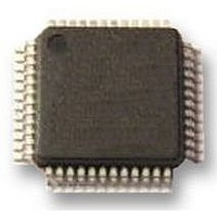
UPD78F0413GA-GAM-AX NEC, UPD78F0413GA-GAM-AX Datasheet - Page 313

UPD78F0413GA-GAM-AX
Manufacturer Part Number
UPD78F0413GA-GAM-AX
Description
8BIT UC, 32K FLASH, 1KB RAM, LCD
Manufacturer
NEC
Datasheet
1.UPD78F0413GA-GAM-AX.pdf
(562 pages)
Specifications of UPD78F0413GA-GAM-AX
Controller Family/series
UPD78F
No. Of I/o's
30
Ram Memory Size
1024Byte
Cpu Speed
10MHz
No. Of Timers
8
No. Of Pwm
RoHS Compliant
Core Size
8bit
Program Memory Size
32KB
Oscillator Type
External, Internal
Available stocks
Company
Part Number
Manufacturer
Quantity
Price
Company:
Part Number:
UPD78F0413GA-GAM-AX
Manufacturer:
ADI
Quantity:
882
Company:
Part Number:
UPD78F0413GA-GAM-AX
Manufacturer:
Renesas Electronics America
Quantity:
10 000
- Current page: 313 of 562
- Download datasheet (4Mb)
13.1 Functions of Serial Interface UART0
(1) Operation stop mode
(2) Asynchronous serial interface (UART) mode
Serial interface UART0 has the following two modes.
This mode is used when serial communication is not executed and can enable a reduction in the power
consumption.
For details, see 13.4.1 Operation stop mode.
The functions of this mode are outlined below.
For details, see 13.4.2
generator.
Cautions 1. If clock supply to serial interface UART0 is not stopped (e.g., in the HALT mode), normal
Maximum transfer rate: 625 kbps
Two-pin configuration
Length of communication data can be selected from 7 or 8 bits.
Dedicated on-chip 5-bit baud rate generator allowing any baud rate to be set
Transmission and reception can be performed independently (full-duplex operation).
Fixed to LSB-first communication
2. Set POWER0 = 1 and then set TXE0 = 1 (transmission) or RXE0 = 1 (reception) to start
3. TXE0 and RXE0 are synchronized by the base clock (f
4. Set transmit data to TXS0 at least one base clock (f
operation continues. If clock supply to serial interface UART0 is stopped (e.g., in the STOP
mode), each register stops operating, and holds the value immediately before clock supply
was stopped. The T
stopped and outputs it. However, the operation is not guaranteed after clock supply is
resumed. Therefore, reset the circuit so that POWER0 = 0, RXE0 = 0, and TXE0 = 0.
communication.
transmission or reception again, set TXE0 or RXE0 to 1 at least two clocks of base clock
after TXE0 or RXE0 has been cleared to 0. If TXE0 or RXE0 is set within two clocks of base
clock, the transmission circuit or reception circuit may not be initialized.
Asynchronous serial interface (UART) mode and 13.4.3
T
R
CHAPTER 13 SERIAL INTERFACE UART0
X
X
D0: Transmit data output pin
D0: Receive data input pin
X
D0 pin also holds the value immediately before clock supply was
User’s Manual U18698EJ1V0UD
XCLK0
) after setting TXE0 = 1.
XCLK0
) set by BRGC0. To enable
Dedicated baud rate
313
Related parts for UPD78F0413GA-GAM-AX
Image
Part Number
Description
Manufacturer
Datasheet
Request
R

Part Number:
Description:
16/8 bit single-chip microcomputer
Manufacturer:
NEC
Datasheet:

Part Number:
Description:
Dual audio power amp circuit
Manufacturer:
NEC
Datasheet:

Part Number:
Description:
Dual comparator
Manufacturer:
NEC
Datasheet:

Part Number:
Description:
MOS type composite field effect transistor
Manufacturer:
NEC
Datasheet:

Part Number:
Description:
50 V/100 mA FET array incorporating 2 N-ch MOSFETs
Manufacturer:
NEC
Datasheet:

Part Number:
Description:
6-pin small MM high-frequency double transistor
Manufacturer:
NEC
Datasheet:

Part Number:
Description:
6-pin small MM high-frequency double transistor
Manufacturer:
NEC
Datasheet:

Part Number:
Description:
6-pin small MM high-frequency double transistor
Manufacturer:
NEC
Datasheet:

Part Number:
Description:
6-pin small MM high-frequency double transistor
Manufacturer:
NEC
Datasheet:

Part Number:
Description:
Twin transistors equipped with different model chips(6P small MM)
Manufacturer:
NEC
Datasheet:

Part Number:
Description:
Bipolar analog integrated circuit
Manufacturer:
NEC
Datasheet:


