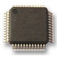
UPD78F0413GA-GAM-AX NEC, UPD78F0413GA-GAM-AX Datasheet - Page 506

UPD78F0413GA-GAM-AX
Manufacturer Part Number
UPD78F0413GA-GAM-AX
Description
8BIT UC, 32K FLASH, 1KB RAM, LCD
Manufacturer
NEC
Datasheet
1.UPD78F0413GA-GAM-AX.pdf
(562 pages)
Specifications of UPD78F0413GA-GAM-AX
Controller Family/series
UPD78F
No. Of I/o's
30
Ram Memory Size
1024Byte
Cpu Speed
10MHz
No. Of Timers
8
No. Of Pwm
RoHS Compliant
Core Size
8bit
Program Memory Size
32KB
Oscillator Type
External, Internal
Available stocks
Company
Part Number
Manufacturer
Quantity
Price
Company:
Part Number:
UPD78F0413GA-GAM-AX
Manufacturer:
ADI
Quantity:
882
Company:
Part Number:
UPD78F0413GA-GAM-AX
Manufacturer:
Renesas Electronics America
Quantity:
10 000
- Current page: 506 of 562
- Download datasheet (4Mb)
506
Address: 0081H/1081H
Address: 0082H/1082H, 0083H/1083H
Address: 0084H/1084H
Notes 1.
Caution Be sure to clear bits 7 to 1 to “0”.
Note Be sure to set 00H to 0082H and 0083H, as these addresses are reserved areas. Also set 00H to 1082H
Note To use the on-chip debug function, set 02H or 03H to 0084H. Set a value that is the same as that of 0084H
Remark For the on-chip debug security ID, see CHAPTER 25 ON-CHIP DEBUG FUNCTION.
and 1083H because 0082H and 0083H are switched with 1082H and 1083H when the boot swap operation
is used.
to 1084H because 0084H and 1084H are switched during the boot swap operation.
2.
POCMODE
POCMODE can only be written by using a dedicated flash memory programmer. It cannot be set
during self-programming or boot swap operation during self-programming (at this time, 1.59 V POC
mode (default) is set). However, because the value of 1081H is copied to 0081H during the boot swap
operation, it is recommended to set a value that is the same as that of 0081H to 1081H when the boot
swap function is used.
To change the setting for the POC mode, set the value to 0081H again after batch erasure (chip
erasure) of the flash memory. The setting cannot be changed after the memory of the specified block
is erased.
OCDEN1
7
0
0
1
7
0
7
0
0
0
1
1
Notes 1, 2
Note
1.59 V POC mode (default)
2.7 V/1.59 V POC mode
OCDEN0
6
0
6
0
6
0
0
1
0
1
Note
Figure 23-1. Format of Option Byte (2/2)
Operation disabled
Setting prohibited
Operation enabled. Does not erase data of the flash memory in case authentication
of the on-chip debug security ID fails.
Operation enabled. Erases data of the flash memory in case authentication of the
on-chip debug security ID fails.
CHAPTER 23 OPTION BYTE
5
0
5
0
5
0
User’s Manual U18698EJ1V0UD
4
0
4
0
4
0
POC mode selection
On-chip debug operation control
3
0
3
0
3
0
2
0
2
0
2
0
OCDEN1
1
0
1
0
1
POCMODE
OCDEN0
0
0
0
0
Related parts for UPD78F0413GA-GAM-AX
Image
Part Number
Description
Manufacturer
Datasheet
Request
R

Part Number:
Description:
16/8 bit single-chip microcomputer
Manufacturer:
NEC
Datasheet:

Part Number:
Description:
Dual audio power amp circuit
Manufacturer:
NEC
Datasheet:

Part Number:
Description:
Dual comparator
Manufacturer:
NEC
Datasheet:

Part Number:
Description:
MOS type composite field effect transistor
Manufacturer:
NEC
Datasheet:

Part Number:
Description:
50 V/100 mA FET array incorporating 2 N-ch MOSFETs
Manufacturer:
NEC
Datasheet:

Part Number:
Description:
6-pin small MM high-frequency double transistor
Manufacturer:
NEC
Datasheet:

Part Number:
Description:
6-pin small MM high-frequency double transistor
Manufacturer:
NEC
Datasheet:

Part Number:
Description:
6-pin small MM high-frequency double transistor
Manufacturer:
NEC
Datasheet:

Part Number:
Description:
6-pin small MM high-frequency double transistor
Manufacturer:
NEC
Datasheet:

Part Number:
Description:
Twin transistors equipped with different model chips(6P small MM)
Manufacturer:
NEC
Datasheet:

Part Number:
Description:
Bipolar analog integrated circuit
Manufacturer:
NEC
Datasheet:


