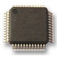
UPD78F0413GA-GAM-AX NEC, UPD78F0413GA-GAM-AX Datasheet - Page 351

UPD78F0413GA-GAM-AX
Manufacturer Part Number
UPD78F0413GA-GAM-AX
Description
8BIT UC, 32K FLASH, 1KB RAM, LCD
Manufacturer
NEC
Datasheet
1.UPD78F0413GA-GAM-AX.pdf
(562 pages)
Specifications of UPD78F0413GA-GAM-AX
Controller Family/series
UPD78F
No. Of I/o's
30
Ram Memory Size
1024Byte
Cpu Speed
10MHz
No. Of Timers
8
No. Of Pwm
RoHS Compliant
Core Size
8bit
Program Memory Size
32KB
Oscillator Type
External, Internal
Available stocks
Company
Part Number
Manufacturer
Quantity
Price
Company:
Part Number:
UPD78F0413GA-GAM-AX
Manufacturer:
ADI
Quantity:
882
Company:
Part Number:
UPD78F0413GA-GAM-AX
Manufacturer:
Renesas Electronics America
Quantity:
10 000
- Current page: 351 of 562
- Download datasheet (4Mb)
Symbol
Address: FF20H
(9) Port mode register 1 (PM1)
(8) Port function register 1 (PF1)
PF1
Caution
This register sets port 1 input/output in 1-bit units.
When using the P13/TxD0/KR4/TxD6 pin for serial interface data output, clear PM13 to 0. The output latch of
P13 at this time may be 0 or 1.
When using the P12/RxD0/KR3/R
this time may be 0 or 1.
PM1 can be set by a 1-bit or 8-bit memory manipulation instruction.
Reset signal generation sets this register to FFH.
Address: FF21H
Symbol
PM1
This register sets the pin functions of P13/TxD0/KR4/TxD6 pin.
PF1 is set using a 1-bit or 8-bit memory manipulation instruction.
Reset signal generation sets PF1 to 00H.
PF13
0
1
7
0
When using the P113/SEG7/RxD6 pin as the P113 or RxD6 pin, set PF11ALL to 0 and ISC3 to 1,
after release of reset.
When using the P113/SEG7/RxD6 pin as the SEG7 pin, set PF11ALL to 1 and ISC3 to 0, after
release of reset.
After reset:
PM1n
7
1
0
1
Used as P13 or KR4
Used as TxD0 or TxD6
After reset: FFH
Output mode (output buffer on)
Input mode (output buffer off)
6
0
00H
Figure 14-12. Format of Port Function Register 1 (PF1)
6
1
Figure 14-13. Format of Port Mode Register 1 (PM1)
R/W
CHAPTER 14 SERIAL INTERFACE UART6
Port (P13), key interrupt (KR4), UART0, UART6 output specification
X
D6 pin for serial interface data input, set PM12 to 1. The output latch of P12 at
5
0
5
1
R/W
User’s Manual U18698EJ1V0UD
P1n pin I/O mode selection (n = 2, 3)
4
1
4
0
PM13
3
PF13
3
PM12
2
2
0
1
1
0
1
1
0
0
0
351
Related parts for UPD78F0413GA-GAM-AX
Image
Part Number
Description
Manufacturer
Datasheet
Request
R

Part Number:
Description:
16/8 bit single-chip microcomputer
Manufacturer:
NEC
Datasheet:

Part Number:
Description:
Dual audio power amp circuit
Manufacturer:
NEC
Datasheet:

Part Number:
Description:
Dual comparator
Manufacturer:
NEC
Datasheet:

Part Number:
Description:
MOS type composite field effect transistor
Manufacturer:
NEC
Datasheet:

Part Number:
Description:
50 V/100 mA FET array incorporating 2 N-ch MOSFETs
Manufacturer:
NEC
Datasheet:

Part Number:
Description:
6-pin small MM high-frequency double transistor
Manufacturer:
NEC
Datasheet:

Part Number:
Description:
6-pin small MM high-frequency double transistor
Manufacturer:
NEC
Datasheet:

Part Number:
Description:
6-pin small MM high-frequency double transistor
Manufacturer:
NEC
Datasheet:

Part Number:
Description:
6-pin small MM high-frequency double transistor
Manufacturer:
NEC
Datasheet:

Part Number:
Description:
Twin transistors equipped with different model chips(6P small MM)
Manufacturer:
NEC
Datasheet:

Part Number:
Description:
Bipolar analog integrated circuit
Manufacturer:
NEC
Datasheet:


