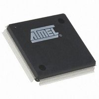
AT91RM9200-QU-002 Atmel, AT91RM9200-QU-002 Datasheet - Page 162

AT91RM9200-QU-002
Manufacturer Part Number
AT91RM9200-QU-002
Description
IC ARM9 MCU 208 PQFP
Manufacturer
Atmel
Series
AT91SAMr
Datasheets
1.AT91RM9200-EK.pdf
(41 pages)
2.AT91RM9200-QU-002.pdf
(701 pages)
3.AT91RM9200-QU-002.pdf
(38 pages)
Specifications of AT91RM9200-QU-002
Core Processor
ARM9
Core Size
16/32-Bit
Speed
180MHz
Connectivity
EBI/EMI, Ethernet, I²C, MMC, SPI, SSC, UART/USART, USB
Peripherals
POR
Number Of I /o
122
Program Memory Size
128KB (128K x 8)
Program Memory Type
ROM
Ram Size
48K x 8
Voltage - Supply (vcc/vdd)
1.65 V ~ 1.95 V
Oscillator Type
Internal
Operating Temperature
-40°C ~ 85°C
Package / Case
208-MQFP, 208-PQFP
Processor Series
AT91Rx
Core
ARM7TDMI
Data Bus Width
32 bit
Data Ram Size
16 KB
Interface Type
2-Wire, EBI, I2S, SPI, UART, USART
Maximum Clock Frequency
180 MHz
Number Of Programmable I/os
122
Number Of Timers
10 bit
Operating Supply Voltage
3 V to 3.6 V
Maximum Operating Temperature
+ 85 C
Mounting Style
SMD/SMT
3rd Party Development Tools
JTRACE-ARM-2M, MDK-ARM, RL-ARM, ULINK2
Development Tools By Supplier
AT91SAM-ICE, AT91-ISP, AT91RM9200-EK
Minimum Operating Temperature
- 40 C
Eeprom Memory
0 Bytes
Input Output
122
Interface
EBI/EMI, UART/USART
Ios
122
Memory Type
ROM
Number Of Bits
32
Package Type
208-pin PQFP
Programmable Memory
128K Bytes
Timers
3-16-bit
Voltage, Range
1.65-1.95 V
Cpu Family
91R
Device Core
ARM920T
Device Core Size
32b
Frequency (max)
180MHz
Total Internal Ram Size
16KB
# I/os (max)
122
Number Of Timers - General Purpose
6
Operating Supply Voltage (typ)
1.8/3.3V
Operating Supply Voltage (max)
1.95/3.6V
Operating Supply Voltage (min)
1.65/3V
Instruction Set Architecture
RISC
Operating Temp Range
-40C to 85C
Operating Temperature Classification
Industrial
Mounting
Surface Mount
Pin Count
208
For Use With
AT91SAM-ICE - EMULATOR FOR AT91 ARM7/ARM9
Lead Free Status / RoHS Status
Lead free / RoHS Compliant
Eeprom Size
-
Data Converters
-
Lead Free Status / Rohs Status
Lead free / RoHS Compliant
Available stocks
Company
Part Number
Manufacturer
Quantity
Price
Company:
Part Number:
AT91RM9200-QU-002
Manufacturer:
COSMO
Quantity:
12 000
Company:
Part Number:
AT91RM9200-QU-002
Manufacturer:
Atmel
Quantity:
1 680
Company:
Part Number:
AT91RM9200-QU-002
Manufacturer:
ATMEL
Quantity:
2 350
Part Number:
AT91RM9200-QU-002
Manufacturer:
ATMEL/爱特梅尔
Quantity:
20 000
Company:
Part Number:
AT91RM9200-QU-002-CQ
Manufacturer:
Atmel
Quantity:
3
- Current page: 162 of 701
- Download datasheet (10Mb)
18.6.3
18.6.3.1
18.6.3.2
Figure 18-11. Standard Read Protocol
18.6.3.3
162
AT91RM9200
Read Access
Read Protocols
Standard Read Protocol
Early Read Protocol
The SMC provides two alternative protocols for external memory read accesses: standard and
early read. The difference between the two protocols lies in the behavior of the NRD signal.
For write accesses, in both protocols, NWE has the same behavior. In the second half of the
master clock cycle, NWE always goes low (see
The protocol is selected by the DRP field in SMC_CSR
page
Note:
Standard read protocol implements a read cycle during which NRD and NWE are similar. Both
are active during the second half of the clock cycle. The first half of the clock cycle allows time to
ensure completion of the previous access as well as the output of address lines and NCS before
the read cycle begins.
During a standard read protocol, NCS is set low and address lines are valid at the beginning of
the external memory access, while NRD goes low only in the second half of the master clock
cycle to avoid bus conflict. See
Early read protocol provides more time for a read access from the memory by asserting NRD at
the beginning of the clock cycle. In the case of successive read cycles in the same memory,
NRD remains active continuously. Since a read cycle normally limits the speed of operation of
the external memory system, early read protocol can allow a faster clock frequency to be used.
However, an extra wait state is required in some cases to avoid contentions on the external bus.
190.). Standard read protocol is the default protocol after reset.
In the following waveforms and descriptions NWE represents NWE, NWR0 and NWR1 unless
NWR0 and NWR1 are otherwise represented. In addition, NCS represents NCS[7:0] (see
“I/O Lines” on page
D[15:0]
A[22:0]
MCK
NRD
NCS
157,
Table 18-1
Figure
18-11.
and
Table
Figure 18-18 on page
18-2).
(See “SMC Chip Select Registers” on
167).
1768I–ATARM–09-Jul-09
18.5.1
Related parts for AT91RM9200-QU-002
Image
Part Number
Description
Manufacturer
Datasheet
Request
R

Part Number:
Description:
Manufacturer:
ATMEL Corporation
Datasheet:

Part Number:
Description:
IC ARM MCU 16BIT 128K 256BGA
Manufacturer:
Atmel
Datasheet:

Part Number:
Description:
IC ARM9 MCU 208 PQFP
Manufacturer:
Atmel
Datasheet:

Part Number:
Description:
DEVEL KIT
Manufacturer:
Atmel
Datasheet:

Part Number:
Description:
KIT DEVELOPMENT AT91RM9200
Manufacturer:
Atmel
Datasheet:

Part Number:
Description:
IC ARM9 MCU 256 BGA
Manufacturer:
Atmel
Datasheet:

Part Number:
Description:
IC ARM MCU 16BIT 128K 208PQFP
Manufacturer:
Atmel
Datasheet:

Part Number:
Description:
AT91RM9200 Development Kit
Manufacturer:
ATMEL Corporation
Datasheet:

Part Number:
Description:
DEV KIT FOR AVR/AVR32
Manufacturer:
Atmel
Datasheet:

Part Number:
Description:
INTERVAL AND WIPE/WASH WIPER CONTROL IC WITH DELAY
Manufacturer:
ATMEL Corporation
Datasheet:

Part Number:
Description:
Low-Voltage Voice-Switched IC for Hands-Free Operation
Manufacturer:
ATMEL Corporation
Datasheet:

Part Number:
Description:
MONOLITHIC INTEGRATED FEATUREPHONE CIRCUIT
Manufacturer:
ATMEL Corporation
Datasheet:

Part Number:
Description:
AM-FM Receiver IC U4255BM-M
Manufacturer:
ATMEL Corporation
Datasheet:


