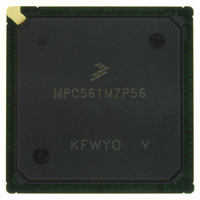
MPC561MZP56 Freescale Semiconductor, MPC561MZP56 Datasheet - Page 1319

MPC561MZP56
Manufacturer Part Number
MPC561MZP56
Description
IC MPU 32BIT 56MHZ PPC 388-PBGA
Manufacturer
Freescale Semiconductor
Series
MPC5xxr
Datasheet
1.MPC561MZP56.pdf
(1420 pages)
Specifications of MPC561MZP56
Core Processor
PowerPC
Core Size
32-Bit
Speed
56MHz
Connectivity
CAN, EBI/EMI, SCI, SPI, UART/USART
Peripherals
POR, PWM, WDT
Number Of I /o
64
Program Memory Type
ROMless
Ram Size
32K x 8
Voltage - Supply (vcc/vdd)
2.5 V ~ 2.7 V
Data Converters
A/D 32x10b
Oscillator Type
External
Operating Temperature
-40°C ~ 125°C
Package / Case
388-BGA
Controller Family/series
POWER 5xx
No. Of I/o's
56
Ram Memory Size
31KB
Cpu Speed
56MHz
No. Of Timers
32
Embedded Interface Type
QSPI, SCI, UART
No. Of Pwm Channels
12
Rohs Compliant
No
Processor Series
MPC5xx
Core
PowerPC
Data Bus Width
32 bit
Data Ram Size
32 KB
Interface Type
CAN, JTAG, QSPI, SCI, SPI, UART
Maximum Clock Frequency
40 MHz
Number Of Programmable I/os
56
Number Of Timers
22
Operating Supply Voltage
2.6 V to 5 V
Maximum Operating Temperature
+ 85 C
Mounting Style
SMD/SMT
Minimum Operating Temperature
- 40 C
On-chip Adc
2 (10 bit, 32 Channel)
For Use With
MPC564EVB - KIT EVAL FOR MPC561/562/563/564
Lead Free Status / RoHS Status
Contains lead / RoHS non-compliant
Eeprom Size
-
Program Memory Size
-
Lead Free Status / Rohs Status
No
Available stocks
Company
Part Number
Manufacturer
Quantity
Price
Company:
Part Number:
MPC561MZP56
Manufacturer:
Freescale Semiconductor
Quantity:
10 000
Company:
Part Number:
MPC561MZP56R2
Manufacturer:
Freescale Semiconductor
Quantity:
10 000
- Current page: 1319 of 1420
- Download datasheet (11Mb)
There are two power-up/down options. Choosing which one is required for an application will depend
upon circuitry connected to 2.6-V compliant pins and dual 2.6-V/5-V compliant pins. Power-up/down
option A is required if 2.6-V compliant pins and dual 2.6-V/5-V compliant pins are connected to the 5-V
supply with a pull-up resistor or driven by 5-V logic during power-up/down. In applications for which this
scenario is not true the power-up/down option B may be implemented. Option B is less stringent and easier
to ensure over a variety of applications.
Refer to
The power consumption during power-up/down sequencing will stay below the operating power
consumption specifications when following these guidelines.
G.9.1
The Option A power-up sequence (excluding V
The first step in the sequence is required is due to gate-to-drain stress limits for transistors in the pads of
2.6-V compliant pins and dual 2.6-V/5-V compliant pins. Damage can occur if gate-to-drain voltage
potential is greater than 3.1 V. This is only a concern at power-up/down. The second step in the sequence
is required is due to ESD diodes in the pad logic for dual 2.6-V/5-V compliant pins and 2.6-V pins. The
diodes are forward biased when V
Figure G-1
power-up sequence if a keep-alive supply is required. The keep-alive supply should be powered-up at the
same instant or before both the high voltage and low voltage supplies are powered-up.
Freescale Semiconductor
1. V
2. V
Table 2-1
DDH
DDH
illustrates the power-up sequence if no keep-alive supply is required.
Power-Up/Down Option A
≤
≥
The V
rate less that 25V/ms.
V
V
DDL
DDL
Figure G-1. Option A Power-Up Sequence Without Keep-Alive Supply
for a list of 2.6 V and dual 2.6V/5 V compliant pins.
DDH
+ 3.1 V (V
- 0.5 V (V
V
V
DDH
DDH
ramp voltage should be kept below 50V/ms and the V
cannot lead V
cannot lag V
DDH
MPC561/MPC563 Reference Manual, Rev. 1.2
DDH
DDL
cannot lag V
cannot lead V
DDL
is greater than V
DDL
by more than 0.5 V
by more than 3.1 V
3.1-V lead
DDKA
DDL
DDL
NOTE:
0.5-V lag
) is
by more than 0.5 V)
DDH
by more than 3.1 V)
and will start to conduct current.
66-MHz Electrical Characteristics
DDL
Figure G-2
V
V
DDH
DDL
ramp
illustrates the
G-13
Related parts for MPC561MZP56
Image
Part Number
Description
Manufacturer
Datasheet
Request
R

Part Number:
Description:
MPC5 1K0 5%
Manufacturer:
TE Connectivity
Datasheet:

Part Number:
Description:
MPC5 500R 5%
Manufacturer:
TE Connectivity
Datasheet:

Part Number:
Description:
MPC5 5K0 5%
Manufacturer:
Tyco Electronics
Datasheet:

Part Number:
Description:
MPC5 5R0 5%
Manufacturer:
Tyco Electronics
Datasheet:

Part Number:
Description:
MPC5 50K 5%
Manufacturer:
Tyco Electronics
Datasheet:

Part Number:
Description:
MPC5 1R0 5%
Manufacturer:
Tyco Electronics
Datasheet:
Part Number:
Description:
Manufacturer:
Freescale Semiconductor, Inc
Datasheet:
Part Number:
Description:
Manufacturer:
Freescale Semiconductor, Inc
Datasheet:
Part Number:
Description:
Manufacturer:
Freescale Semiconductor, Inc
Datasheet:
Part Number:
Description:
Manufacturer:
Freescale Semiconductor, Inc
Datasheet:
Part Number:
Description:
Manufacturer:
Freescale Semiconductor, Inc
Datasheet:


