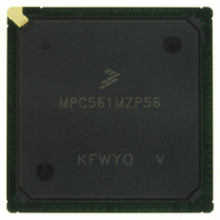
MPC561MZP56 Freescale Semiconductor, MPC561MZP56 Datasheet - Page 432

MPC561MZP56
Manufacturer Part Number
MPC561MZP56
Description
IC MPU 32BIT 56MHZ PPC 388-PBGA
Manufacturer
Freescale Semiconductor
Series
MPC5xxr
Datasheet
1.MPC561MZP56.pdf
(1420 pages)
Specifications of MPC561MZP56
Core Processor
PowerPC
Core Size
32-Bit
Speed
56MHz
Connectivity
CAN, EBI/EMI, SCI, SPI, UART/USART
Peripherals
POR, PWM, WDT
Number Of I /o
64
Program Memory Type
ROMless
Ram Size
32K x 8
Voltage - Supply (vcc/vdd)
2.5 V ~ 2.7 V
Data Converters
A/D 32x10b
Oscillator Type
External
Operating Temperature
-40°C ~ 125°C
Package / Case
388-BGA
Controller Family/series
POWER 5xx
No. Of I/o's
56
Ram Memory Size
31KB
Cpu Speed
56MHz
No. Of Timers
32
Embedded Interface Type
QSPI, SCI, UART
No. Of Pwm Channels
12
Rohs Compliant
No
Processor Series
MPC5xx
Core
PowerPC
Data Bus Width
32 bit
Data Ram Size
32 KB
Interface Type
CAN, JTAG, QSPI, SCI, SPI, UART
Maximum Clock Frequency
40 MHz
Number Of Programmable I/os
56
Number Of Timers
22
Operating Supply Voltage
2.6 V to 5 V
Maximum Operating Temperature
+ 85 C
Mounting Style
SMD/SMT
Minimum Operating Temperature
- 40 C
On-chip Adc
2 (10 bit, 32 Channel)
For Use With
MPC564EVB - KIT EVAL FOR MPC561/562/563/564
Lead Free Status / RoHS Status
Contains lead / RoHS non-compliant
Eeprom Size
-
Program Memory Size
-
Lead Free Status / Rohs Status
No
Available stocks
Company
Part Number
Manufacturer
Quantity
Price
Company:
Part Number:
MPC561MZP56
Manufacturer:
Freescale Semiconductor
Quantity:
10 000
Company:
Part Number:
MPC561MZP56R2
Manufacturer:
Freescale Semiconductor
Quantity:
10 000
- Current page: 432 of 1420
- Download datasheet (11Mb)
Memory Controller
10.9.4
10-34
1,
Bits
30
31
1
It is recommended that this field hold values that are the power of 2 minus 1 (e.g., 2
HRESET
HRESET
Memory Controller Option Registers (OR0–OR3)
Field
Addr
Name
BI
V
MSB
AM
16
0
Burst inhibit
0 Memory controller drives BI negated (high). The bank supports burst accesses.
1 Memory controller drives BI asserted (low). The bank does not support burst accesses.
NOTE: Following a system reset, the BI bit is set.
Valid bit. When set, this bit indicates that the contents of the base-register and option-register
pair are valid. The CS signal does not assert until the V-bit is set.
NOTE: An access to a region that has no V-bit set may cause a bus monitor timeout. See
Table 10-9
Figure 10-24. Memory Controller Option Registers 1–3 (OR0–OR3)
17
1
Branch Register
0x2F C104 (OR0); 0x2F C10C (OR1); 0x2F C114 (OR2), 0x2F C11C (OR3)
Table 10-8. BR0–BR3 Bit Descriptions (continued)
ATM
18
2
BR0
BR1
BR2
BR3
for the reset value of this bit in BR0.
MPC561/MPC563 Reference Manual, Rev. 1.2
19
3
0000_0000
Table 10-9. BRx[V] Reset Value
CSNT
20
4
21
5
ACS
0000_0000_0000_0000
22
6
EHTR
23
7
Description
AM
1
24
8
BRx[V] Reset Value
25
ID20 & ID31
9
1111
SCY
ID3
10
26
0
0
11
27
3
- 1 = 7 [0b111]).
12
28
0
BSCY
Freescale Semiconductor
13
29
1
14
30
1
TRLX
LSB
15
31
0
Related parts for MPC561MZP56
Image
Part Number
Description
Manufacturer
Datasheet
Request
R

Part Number:
Description:
MPC5 1K0 5%
Manufacturer:
TE Connectivity
Datasheet:

Part Number:
Description:
MPC5 500R 5%
Manufacturer:
TE Connectivity
Datasheet:

Part Number:
Description:
MPC5 5K0 5%
Manufacturer:
Tyco Electronics
Datasheet:

Part Number:
Description:
MPC5 5R0 5%
Manufacturer:
Tyco Electronics
Datasheet:

Part Number:
Description:
MPC5 50K 5%
Manufacturer:
Tyco Electronics
Datasheet:

Part Number:
Description:
MPC5 1R0 5%
Manufacturer:
Tyco Electronics
Datasheet:
Part Number:
Description:
Manufacturer:
Freescale Semiconductor, Inc
Datasheet:
Part Number:
Description:
Manufacturer:
Freescale Semiconductor, Inc
Datasheet:
Part Number:
Description:
Manufacturer:
Freescale Semiconductor, Inc
Datasheet:
Part Number:
Description:
Manufacturer:
Freescale Semiconductor, Inc
Datasheet:
Part Number:
Description:
Manufacturer:
Freescale Semiconductor, Inc
Datasheet:


