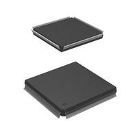
HD6417750SF200V Renesas Electronics America, HD6417750SF200V Datasheet - Page 620

HD6417750SF200V
Manufacturer Part Number
HD6417750SF200V
Description
MPU 3V 16K PB-FREE 208-QFP
Manufacturer
Renesas Electronics America
Series
SuperH® SH7750r
Datasheet
1.D6417750RBP240DV.pdf
(1164 pages)
Specifications of HD6417750SF200V
Core Processor
SH-4
Core Size
32-Bit
Speed
200MHz
Connectivity
EBI/EMI, FIFO, SCI, SmartCard
Peripherals
DMA, POR, WDT
Number Of I /o
28
Program Memory Type
ROMless
Ram Size
24K x 8
Voltage - Supply (vcc/vdd)
1.8 V ~ 2.07 V
Oscillator Type
External
Operating Temperature
-20°C ~ 75°C
Package / Case
208-QFP
Lead Free Status / RoHS Status
Lead free / RoHS Compliant
Eeprom Size
-
Program Memory Size
-
Data Converters
-
Available stocks
Company
Part Number
Manufacturer
Quantity
Price
Company:
Part Number:
HD6417750SF200V
Manufacturer:
Renesas Electronics America
Quantity:
10 000
- Current page: 620 of 1164
- Download datasheet (7Mb)
Section 13 Bus State Controller (BSC)
13.3.10 Waits between Access Cycles
A problem associated with higher external memory bus operating frequencies is that data buffer
turn-off on completion of a read from a low-speed device may be too slow, causing a collision
with the data in the next access, and so resulting in lower reliability or incorrect operation. To
avoid this problem, a data collision prevention feature has been provided. This memorizes the
preceding access area and the kind of read/write, and if there is a possibility of a bus collision
when the next access is started, inserts a wait cycle before the access cycle to prevent a data
collision. Wait cycle insertion consists of inserting idle cycles between access cycles, as shown in
section 13.2.5, Wait Control Register (WCR1). When this LSI performs consecutive write cycles,
the data transfer direction is fixed (from this LSI to other memory) and there is no problem. With
read accesses to the same area, also, in principle data is output from the same data buffer, and wait
cycle insertion is not performed. If there is originally space between accesses, according to the
setting of bits AnIW2–AnIW0 (n = 0 to 6) in WCR1, the number of idle cycles inserted is the
specified number of idle cycles minus the number of empty cycles.
When bus arbitration is performed, the bus is released after waits are inserted between cycles.
In single address mode DMA transfer, when data transfer is performed from an I/O device to
memory the data on the bus is determined by the speed of the I/O device. With a low-speed I/O
device, an inter-cycle idle wait equivalent to the output buffer turn-off time must be inserted. Even
with high-speed memory, when DMA transfer is considered, it may be necessary to insert an inter-
cycle wait to adjust to the speed of a low-speed device, preventing the memory from being used at
full speed.
Bits DMAIW2–DMAIW0 in wait control register 1 (WCR1) allow an inter-cycle wait setting to
be made when transferring data from an I/O device to memory using single address mode DMA
transfer. From 0 to 15 waits can be inserted. The number of waits specified by DMAIW2–
DMAIW0 are inserted in single address DMA transfers to all areas.
In dual address mode DMA transfer, the normal inter-cycle wait specified by AnIW2–AnIW0 (n =
0 to 6) is inserted.
Rev.7.00 Oct. 10, 2008 Page 534 of 1074
REJ09B0366-0700
Related parts for HD6417750SF200V
Image
Part Number
Description
Manufacturer
Datasheet
Request
R

Part Number:
Description:
KIT STARTER FOR M16C/29
Manufacturer:
Renesas Electronics America
Datasheet:

Part Number:
Description:
KIT STARTER FOR R8C/2D
Manufacturer:
Renesas Electronics America
Datasheet:

Part Number:
Description:
R0K33062P STARTER KIT
Manufacturer:
Renesas Electronics America
Datasheet:

Part Number:
Description:
KIT STARTER FOR R8C/23 E8A
Manufacturer:
Renesas Electronics America
Datasheet:

Part Number:
Description:
KIT STARTER FOR R8C/25
Manufacturer:
Renesas Electronics America
Datasheet:

Part Number:
Description:
KIT STARTER H8S2456 SHARPE DSPLY
Manufacturer:
Renesas Electronics America
Datasheet:

Part Number:
Description:
KIT STARTER FOR R8C38C
Manufacturer:
Renesas Electronics America
Datasheet:

Part Number:
Description:
KIT STARTER FOR R8C35C
Manufacturer:
Renesas Electronics America
Datasheet:

Part Number:
Description:
KIT STARTER FOR R8CL3AC+LCD APPS
Manufacturer:
Renesas Electronics America
Datasheet:

Part Number:
Description:
KIT STARTER FOR RX610
Manufacturer:
Renesas Electronics America
Datasheet:

Part Number:
Description:
KIT STARTER FOR R32C/118
Manufacturer:
Renesas Electronics America
Datasheet:

Part Number:
Description:
KIT DEV RSK-R8C/26-29
Manufacturer:
Renesas Electronics America
Datasheet:

Part Number:
Description:
KIT STARTER FOR SH7124
Manufacturer:
Renesas Electronics America
Datasheet:

Part Number:
Description:
KIT STARTER FOR H8SX/1622
Manufacturer:
Renesas Electronics America
Datasheet:

Part Number:
Description:
KIT DEV FOR SH7203
Manufacturer:
Renesas Electronics America
Datasheet:


