HD6417750SF200V Renesas Electronics America, HD6417750SF200V Datasheet - Page 74
HD6417750SF200V
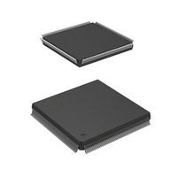
Manufacturer Part Number
HD6417750SF200V
Description
MPU 3V 16K PB-FREE 208-QFP
Manufacturer
Renesas Electronics America
Series
SuperH® SH7750r
Datasheet
1.D6417750RBP240DV.pdf
(1164 pages)
Specifications of HD6417750SF200V
Core Processor
SH-4
Core Size
32-Bit
Speed
200MHz
Connectivity
EBI/EMI, FIFO, SCI, SmartCard
Peripherals
DMA, POR, WDT
Number Of I /o
28
Program Memory Type
ROMless
Ram Size
24K x 8
Voltage - Supply (vcc/vdd)
1.8 V ~ 2.07 V
Oscillator Type
External
Operating Temperature
-20°C ~ 75°C
Package / Case
208-QFP
Lead Free Status / RoHS Status
Lead free / RoHS Compliant
Eeprom Size
-
Program Memory Size
-
Data Converters
-
Available stocks
Company
Part Number
Manufacturer
Quantity
Price
Company:

Part Number:
HD6417750SF200V
Manufacturer:
Renesas Electronics America
Quantity:
10 000


Section 16 Serial Communication Interface with FIFO (SCIF)
Figure 16.1 Block Diagram of SCIF.......................................................................................... 727
Figure 16.2 MD8/RTS2 Pin....................................................................................................... 753
Figure 16.3 CTS2 Pin ................................................................................................................ 754
Figure 16.4 MD1/TxD2 Pin....................................................................................................... 755
Figure 16.5 MD2/RxD2 Pin ...................................................................................................... 755
Figure 16.6 Sample SCIF Initialization Flowchart .................................................................... 761
Figure 16.7 Sample Serial Transmission Flowchart .................................................................. 762
Figure 16.8 Example of Transmit Operation (Example with 8-Bit Data, Parity,
Figure 16.9 Example of Operation Using Modem Control (CTS2)........................................... 764
Figure 16.10 Sample Serial Reception Flowchart (1).................................................................. 765
Figure 16.10 Sample Serial Reception Flowchart (2).................................................................. 766
Figure 16.11 Example of SCIF Receive Operation (Example with 8-Bit Data, Parity,
Figure 16.12 Example of Operation Using Modem Control (RTS2)........................................... 769
Figure 16.13 Receive Data Sampling Timing in Asynchronous Mode ....................................... 772
Figure 16.14 Overrun Error Flag ................................................................................................. 774
Section 17 Smart Card Interface
Figure 17.1 Block Diagram of Smart Card Interface................................................................. 776
Figure 17.2 Schematic Diagram of Smart Card Interface Pin Connections............................... 783
Figure 17.3 Smart Card Interface Data Format ......................................................................... 784
Figure 17.4 TEND Generation Timing...................................................................................... 786
Figure 17.5 Sample Start Character Waveforms ....................................................................... 787
Figure 17.6 Difference in Clock Output According to GM Bit Setting..................................... 790
Figure 17.7 Sample Initialization Flowchart ............................................................................. 791
Figure 17.8 Sample Transmission Processing Flowchart .......................................................... 793
Figure 17.9 Sample Reception Processing Flowchart ............................................................... 795
Figure 17.10 Receive Data Sampling Timing in Smart Card Mode ............................................ 797
Figure 17.11 Retransfer Operation in SCI Receive Mode ........................................................... 799
Figure 17.12 Retransfer Operation in SCI Transmit Mode ......................................................... 799
Figure 17.13 Procedure for Stopping and Restarting the Clock .................................................. 800
Section 18 I/O Ports
Figure 18.1 16-Bit Port.............................................................................................................. 804
Figure 18.2 4-Bit Port................................................................................................................ 805
Figure 18.3 MD0/SCK Pin ........................................................................................................ 806
Figure 18.4 MD7/TxD Pin......................................................................................................... 807
Figure 18.5 RxD Pin.................................................................................................................. 807
Rev.7.00 Oct. 10, 2008 Page lxxii of lxxxiv
REJ09B0366-0700
One Stop Bit).......................................................................................................... 764
One Stop Bit).......................................................................................................... 768
Related parts for HD6417750SF200V
Image
Part Number
Description
Manufacturer
Datasheet
Request
R

Part Number:
Description:
KIT STARTER FOR M16C/29
Manufacturer:
Renesas Electronics America
Datasheet:

Part Number:
Description:
KIT STARTER FOR R8C/2D
Manufacturer:
Renesas Electronics America
Datasheet:

Part Number:
Description:
R0K33062P STARTER KIT
Manufacturer:
Renesas Electronics America
Datasheet:

Part Number:
Description:
KIT STARTER FOR R8C/23 E8A
Manufacturer:
Renesas Electronics America
Datasheet:

Part Number:
Description:
KIT STARTER FOR R8C/25
Manufacturer:
Renesas Electronics America
Datasheet:

Part Number:
Description:
KIT STARTER H8S2456 SHARPE DSPLY
Manufacturer:
Renesas Electronics America
Datasheet:

Part Number:
Description:
KIT STARTER FOR R8C38C
Manufacturer:
Renesas Electronics America
Datasheet:

Part Number:
Description:
KIT STARTER FOR R8C35C
Manufacturer:
Renesas Electronics America
Datasheet:

Part Number:
Description:
KIT STARTER FOR R8CL3AC+LCD APPS
Manufacturer:
Renesas Electronics America
Datasheet:
Part Number:
Description:
KIT STARTER FOR RX610
Manufacturer:
Renesas Electronics America
Datasheet:

Part Number:
Description:
KIT STARTER FOR R32C/118
Manufacturer:
Renesas Electronics America
Datasheet:

Part Number:
Description:
KIT DEV RSK-R8C/26-29
Manufacturer:
Renesas Electronics America
Datasheet:

Part Number:
Description:
KIT STARTER FOR SH7124
Manufacturer:
Renesas Electronics America
Datasheet:

Part Number:
Description:
KIT STARTER FOR H8SX/1622
Manufacturer:
Renesas Electronics America
Datasheet:

Part Number:
Description:
KIT DEV FOR SH7203
Manufacturer:
Renesas Electronics America
Datasheet: