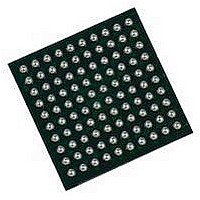
EP3C10M164C8N Altera, EP3C10M164C8N Datasheet - Page 121

EP3C10M164C8N
Manufacturer Part Number
EP3C10M164C8N
Description
IC CYCLONE III FPGA 402MHZ BGA-164
Manufacturer
Altera
Series
Cyclone IIIr
Specifications of EP3C10M164C8N
No. Of Logic Blocks
645
Family Type
Cyclone III
No. Of I/o's
106
I/o Supply Voltage
3.3V
Operating Frequency Max
402MHz
Operating Temperature Range
0°C To +85°C
Family Name
Cyclone III
Number Of Logic Blocks/elements
10320
# I/os (max)
106
Frequency (max)
402MHz
Process Technology
65nm
Operating Supply Voltage (typ)
1.2V
Logic Cells
10320
Ram Bits
423936
Operating Supply Voltage (min)
1.15V
Operating Supply Voltage (max)
1.25V
Operating Temp Range
0C to 85C
Operating Temperature Classification
Commercial
Mounting
Surface Mount
Pin Count
164
Package Type
MBGA
Lead Free Status / RoHS Status
Lead free / RoHS Compliant
Lead Free Status / RoHS Status
Lead free / RoHS Compliant
Available stocks
Company
Part Number
Manufacturer
Quantity
Price
- Current page: 121 of 350
- Download datasheet (8Mb)
Chapter 6: I/O Features in the Cyclone III Device Family
Pad Placement and DC Guidelines
Pad Placement and DC Guidelines
Pad Placement
DC Guidelines
Chapter Revision History
Table 6–7. Chapter Revision History (Part 1 of 3)
© December 2009
December 2009
July 2009
June 2009
October 2008
Date
f
Altera Corporation
Altera recommends that you create a Quartus II design, enter your device I/O
assignments, and compile your design to validate your pin placement. The Quartus II
software checks your pin connections with respect to the I/O assignment and
placement rules to ensure proper device operation. These rules are dependent on
device density, package, I/O assignments, voltage assignments, and other factors that
are not fully described in this chapter.
For more information about how the Quartus II software checks I/O restrictions, refer
to the
For the Quartus II software to automatically check for illegally placed pads according
to the DC guidelines, set the DC current sink or source value to Electromigration
Current assignment on each of the output pins that are connected to the external
resistive load.
The programmable current strength setting has an impact on the amount of DC
current that an output pin can source or sink. Determine if the current strength setting
is sufficient for the external resistive load condition on the output pin.
Table 6–7
Version
3.2
3.1
3.0
2.1
I/O Management
lists the revision history for this chapter.
Minor changes to the text.
Made minor correction to the part number.
Updated to include Cyclone III LS information
■
■
■
■
■
■
■
■
■
Updated chapter part number.
Updated “Introduction” on page 6–1, “PCI-Clamp Diode” on page 6–6, “On-
Chip Series Termination Without Calibration” on page 6–10, “I/O Standards”
on page 6–11, “I/O Banks” on page 6–16, “High-Speed Differential
Interfaces” on page 6–20, and “External Memory Interfacing” on page 6–20.
Updated Table 6–6 on page 6–18.
Added (Note 6) to Table 6–5.
Updated the “I/O Banks” section.
Updated the “Differential Pad Placement Guidelines” section.
Updated the “V
Removed any mention of “RSDS and PPDS are registered trademarks of
National Semiconductor” from chapter.
Updated chapter to new template.
chapter in volume 2 of the Quartus II Handbook.
REF
Pad Placement Guidelines” section.
Changes Made
Cyclone III Device Handbook, Volume 1
6–21
Related parts for EP3C10M164C8N
Image
Part Number
Description
Manufacturer
Datasheet
Request
R

Part Number:
Description:
CYCLONE II STARTER KIT EP2C20N
Manufacturer:
Altera
Datasheet:

Part Number:
Description:
CPLD, EP610 Family, ECMOS Process, 300 Gates, 16 Macro Cells, 16 Reg., 16 User I/Os, 5V Supply, 35 Speed Grade, 24DIP
Manufacturer:
Altera Corporation
Datasheet:

Part Number:
Description:
CPLD, EP610 Family, ECMOS Process, 300 Gates, 16 Macro Cells, 16 Reg., 16 User I/Os, 5V Supply, 15 Speed Grade, 24DIP
Manufacturer:
Altera Corporation
Datasheet:

Part Number:
Description:
Manufacturer:
Altera Corporation
Datasheet:

Part Number:
Description:
CPLD, EP610 Family, ECMOS Process, 300 Gates, 16 Macro Cells, 16 Reg., 16 User I/Os, 5V Supply, 30 Speed Grade, 24DIP
Manufacturer:
Altera Corporation
Datasheet:

Part Number:
Description:
High-performance, low-power erasable programmable logic devices with 8 macrocells, 10ns
Manufacturer:
Altera Corporation
Datasheet:

Part Number:
Description:
High-performance, low-power erasable programmable logic devices with 8 macrocells, 7ns
Manufacturer:
Altera Corporation
Datasheet:

Part Number:
Description:
Classic EPLD
Manufacturer:
Altera Corporation
Datasheet:

Part Number:
Description:
High-performance, low-power erasable programmable logic devices with 8 macrocells, 10ns
Manufacturer:
Altera Corporation
Datasheet:

Part Number:
Description:
Manufacturer:
Altera Corporation
Datasheet:

Part Number:
Description:
Manufacturer:
Altera Corporation
Datasheet:

Part Number:
Description:
Manufacturer:
Altera Corporation
Datasheet:

Part Number:
Description:
CPLD, EP610 Family, ECMOS Process, 300 Gates, 16 Macro Cells, 16 Reg., 16 User I/Os, 5V Supply, 25 Speed Grade, 24DIP
Manufacturer:
Altera Corporation
Datasheet:


