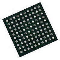
EP3C10M164C8N Altera, EP3C10M164C8N Datasheet - Page 214

EP3C10M164C8N
Manufacturer Part Number
EP3C10M164C8N
Description
IC CYCLONE III FPGA 402MHZ BGA-164
Manufacturer
Altera
Series
Cyclone IIIr
Specifications of EP3C10M164C8N
No. Of Logic Blocks
645
Family Type
Cyclone III
No. Of I/o's
106
I/o Supply Voltage
3.3V
Operating Frequency Max
402MHz
Operating Temperature Range
0°C To +85°C
Family Name
Cyclone III
Number Of Logic Blocks/elements
10320
# I/os (max)
106
Frequency (max)
402MHz
Process Technology
65nm
Operating Supply Voltage (typ)
1.2V
Logic Cells
10320
Ram Bits
423936
Operating Supply Voltage (min)
1.15V
Operating Supply Voltage (max)
1.25V
Operating Temp Range
0C to 85C
Operating Temperature Classification
Commercial
Mounting
Surface Mount
Pin Count
164
Package Type
MBGA
Lead Free Status / RoHS Status
Lead free / RoHS Compliant
Lead Free Status / RoHS Status
Lead free / RoHS Compliant
Available stocks
Company
Part Number
Manufacturer
Quantity
Price
- Current page: 214 of 350
- Download datasheet (8Mb)
9–54
Figure 9–26. JTAG Configuration of Multiple Devices Using a Download Cable (2.5, 3.0, and 3.3-V V
Pins)
Notes to
(1) Connect these pull-up resistors to the V
(2) Connect the nCONFIG and MSEL[3..0] pins to support a non-JTAG configuration scheme. If you only use a JTAG configuration, connect the
(3) Pin 6 of the header is a V
(4) The nCE pin must be connected to ground or driven low for successful JTAG configuration.
(5) Power up the V
Cyclone III Device Handbook, Volume 1
Pin 1
10-Pin Male Header
Download Cable
nCONFIG pin to logic high and the MSEL[3..0] pins to ground. In addition, pull DCLK and DATA[0] either high or low, whichever is
convenient on your board.
MasterBlaster Serial/USB Communications Cable User
ByteBlaster II cables, this pin is connected to nCE when it is used for AS programming, otherwise it is a no connect.
to 2.5 V. Pin 4 of the header is a V
circuit boards, DC power supply, or 5.0 V from the USB cable. For this value, refer to the
Figure
V
CCA
(5)
10 kΩ
VIO
(3)
9–26:
1 kΩ
V
CC
CCA
of the ByteBlaster II, USB-Blaster, or ByteBlasterMV cable with a 2.5- V supply from V
V
CCA
10 kΩ
IO
(2)
(2)
(2)
(2)
(2)
reference voltage for the MasterBlaster output driver. V
V
CCIO
10
CC
(1)
DCLK
nST A TUS
DATA[0]
nCONFIG
MSEL[3..0]
nCEO
nCE
TDI
Chapter 9: Configuration, Design Security, and Remote System Upgrades in the Cyclone III Device Family
kΩ
power supply for the MasterBlaster cable. The MasterBlaster cable can receive power from either 5.0- or 3.3-V
TMS
(4)
Cyclone III Device
CCIO
Family
TCK
CONF_DONE
supply of the bank in which the pin resides.
TDO
V
Guide. In the ByteBlasterMV cable, this pin is a no connect. In the USB-Blaster and
CCIO
10
(1)
kΩ
(2)
(2)
(2)
(2)
(2)
V
CCIO
10
(1)
nST A TUS
DATA[0]
DCLK
nCONFIG
MSEL[3..0]
nCEO
nCE
TDI
kΩ
TMS
Cyclone III Device
(4)
IO
Family
must match the V
CONF_DONE
TCK
MasterBlaster Serial/USB Communications User
TDO
V
CCIO
10
CCA
CCA
(1)
kΩ
of the device. For this value, refer to the
. Third-party programmers must switch
© December 2009 Altera Corporation
(2)
(2)
(2)
(2)
(2)
V
CCIO
10
(1)
nST A TUS
DATA[0]
DCLK
nCONFIG
MSEL[3..0]
nCEO
nCE
TDI
CCIO
kΩ
TMS
(4)
Powering the JTAG
Cyclone III Device
Configuration Features
Family
TCK
CONF_DONE
TDO
V
CCIO
Guide.
10
(1)
kΩ
Related parts for EP3C10M164C8N
Image
Part Number
Description
Manufacturer
Datasheet
Request
R

Part Number:
Description:
CYCLONE II STARTER KIT EP2C20N
Manufacturer:
Altera
Datasheet:

Part Number:
Description:
CPLD, EP610 Family, ECMOS Process, 300 Gates, 16 Macro Cells, 16 Reg., 16 User I/Os, 5V Supply, 35 Speed Grade, 24DIP
Manufacturer:
Altera Corporation
Datasheet:

Part Number:
Description:
CPLD, EP610 Family, ECMOS Process, 300 Gates, 16 Macro Cells, 16 Reg., 16 User I/Os, 5V Supply, 15 Speed Grade, 24DIP
Manufacturer:
Altera Corporation
Datasheet:

Part Number:
Description:
Manufacturer:
Altera Corporation
Datasheet:

Part Number:
Description:
CPLD, EP610 Family, ECMOS Process, 300 Gates, 16 Macro Cells, 16 Reg., 16 User I/Os, 5V Supply, 30 Speed Grade, 24DIP
Manufacturer:
Altera Corporation
Datasheet:

Part Number:
Description:
High-performance, low-power erasable programmable logic devices with 8 macrocells, 10ns
Manufacturer:
Altera Corporation
Datasheet:

Part Number:
Description:
High-performance, low-power erasable programmable logic devices with 8 macrocells, 7ns
Manufacturer:
Altera Corporation
Datasheet:

Part Number:
Description:
Classic EPLD
Manufacturer:
Altera Corporation
Datasheet:

Part Number:
Description:
High-performance, low-power erasable programmable logic devices with 8 macrocells, 10ns
Manufacturer:
Altera Corporation
Datasheet:

Part Number:
Description:
Manufacturer:
Altera Corporation
Datasheet:

Part Number:
Description:
Manufacturer:
Altera Corporation
Datasheet:

Part Number:
Description:
Manufacturer:
Altera Corporation
Datasheet:

Part Number:
Description:
CPLD, EP610 Family, ECMOS Process, 300 Gates, 16 Macro Cells, 16 Reg., 16 User I/Os, 5V Supply, 25 Speed Grade, 24DIP
Manufacturer:
Altera Corporation
Datasheet:


