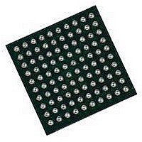
EP3C10M164C8N Altera, EP3C10M164C8N Datasheet - Page 43

EP3C10M164C8N
Manufacturer Part Number
EP3C10M164C8N
Description
IC CYCLONE III FPGA 402MHZ BGA-164
Manufacturer
Altera
Series
Cyclone IIIr
Specifications of EP3C10M164C8N
No. Of Logic Blocks
645
Family Type
Cyclone III
No. Of I/o's
106
I/o Supply Voltage
3.3V
Operating Frequency Max
402MHz
Operating Temperature Range
0°C To +85°C
Family Name
Cyclone III
Number Of Logic Blocks/elements
10320
# I/os (max)
106
Frequency (max)
402MHz
Process Technology
65nm
Operating Supply Voltage (typ)
1.2V
Logic Cells
10320
Ram Bits
423936
Operating Supply Voltage (min)
1.15V
Operating Supply Voltage (max)
1.25V
Operating Temp Range
0C to 85C
Operating Temperature Classification
Commercial
Mounting
Surface Mount
Pin Count
164
Package Type
MBGA
Lead Free Status / RoHS Status
Lead free / RoHS Compliant
Lead Free Status / RoHS Status
Lead free / RoHS Compliant
Available stocks
Company
Part Number
Manufacturer
Quantity
Price
- Current page: 43 of 350
- Download datasheet (8Mb)
Chapter 3: Memory Blocks in the Cyclone III Device Family
Overview
Mixed-Width Support
Asynchronous Clear
© December 2009
1
Altera Corporation
Figure 3–5. Cyclone III Device Family Address Clock Enable During Write Cycle Waveform
M9K memory blocks support mixed data widths. When using simple dual-port, true
dual-port, or FIFO modes, mixed width support allows you to read and write
different data widths to an M9K memory block. For more information about the
different widths supported per memory mode, refer to
page
The Cyclone III device family supports asynchronous clears for read address
registers, output registers, and output latches only. Input registers other than read
address registers are not supported. When applied to output registers, the
asynchronous clear signal clears the output registers and the effects are immediately
seen. If your RAM does not use output registers, you can still clear the RAM outputs
using the output latch asynchronous clear feature.
Asserting asynchronous clear to the read address register during a read operation
might corrupt the memory content.
Figure 3–6
Figure 3–6. Output Latch Asynchronous Clear Waveform
aclr at latch
latched address
(inside memory)
3–8.
contents at a0
contents at a1
contents at a2
contents at a3
contents at a4
contents at a5
addressstall
wraddress
aclr
clk
q
shows the functional waveform for the asynchronous clear feature.
inclock
wren
data
an
XX
a0
00
a1
XX
a0
01
a1
a2
XX
01
02
a2
XX
XX
XX
a1
02
a3
03
00
“Memory Modes” on
Cyclone III Device Handbook, Volume 1
04
a4
a0
a4
03
a5
05
a1
04
a5
05
a6
06
3–7
Related parts for EP3C10M164C8N
Image
Part Number
Description
Manufacturer
Datasheet
Request
R

Part Number:
Description:
CYCLONE II STARTER KIT EP2C20N
Manufacturer:
Altera
Datasheet:

Part Number:
Description:
CPLD, EP610 Family, ECMOS Process, 300 Gates, 16 Macro Cells, 16 Reg., 16 User I/Os, 5V Supply, 35 Speed Grade, 24DIP
Manufacturer:
Altera Corporation
Datasheet:

Part Number:
Description:
CPLD, EP610 Family, ECMOS Process, 300 Gates, 16 Macro Cells, 16 Reg., 16 User I/Os, 5V Supply, 15 Speed Grade, 24DIP
Manufacturer:
Altera Corporation
Datasheet:

Part Number:
Description:
Manufacturer:
Altera Corporation
Datasheet:

Part Number:
Description:
CPLD, EP610 Family, ECMOS Process, 300 Gates, 16 Macro Cells, 16 Reg., 16 User I/Os, 5V Supply, 30 Speed Grade, 24DIP
Manufacturer:
Altera Corporation
Datasheet:

Part Number:
Description:
High-performance, low-power erasable programmable logic devices with 8 macrocells, 10ns
Manufacturer:
Altera Corporation
Datasheet:

Part Number:
Description:
High-performance, low-power erasable programmable logic devices with 8 macrocells, 7ns
Manufacturer:
Altera Corporation
Datasheet:

Part Number:
Description:
Classic EPLD
Manufacturer:
Altera Corporation
Datasheet:

Part Number:
Description:
High-performance, low-power erasable programmable logic devices with 8 macrocells, 10ns
Manufacturer:
Altera Corporation
Datasheet:

Part Number:
Description:
Manufacturer:
Altera Corporation
Datasheet:

Part Number:
Description:
Manufacturer:
Altera Corporation
Datasheet:

Part Number:
Description:
Manufacturer:
Altera Corporation
Datasheet:

Part Number:
Description:
CPLD, EP610 Family, ECMOS Process, 300 Gates, 16 Macro Cells, 16 Reg., 16 User I/Os, 5V Supply, 25 Speed Grade, 24DIP
Manufacturer:
Altera Corporation
Datasheet:


