EP3C10M164C8N Altera, EP3C10M164C8N Datasheet - Page 311
EP3C10M164C8N
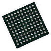
Manufacturer Part Number
EP3C10M164C8N
Description
IC CYCLONE III FPGA 402MHZ BGA-164
Manufacturer
Altera
Series
Cyclone IIIr
Specifications of EP3C10M164C8N
No. Of Logic Blocks
645
Family Type
Cyclone III
No. Of I/o's
106
I/o Supply Voltage
3.3V
Operating Frequency Max
402MHz
Operating Temperature Range
0°C To +85°C
Family Name
Cyclone III
Number Of Logic Blocks/elements
10320
# I/os (max)
106
Frequency (max)
402MHz
Process Technology
65nm
Operating Supply Voltage (typ)
1.2V
Logic Cells
10320
Ram Bits
423936
Operating Supply Voltage (min)
1.15V
Operating Supply Voltage (max)
1.25V
Operating Temp Range
0C to 85C
Operating Temperature Classification
Commercial
Mounting
Surface Mount
Pin Count
164
Package Type
MBGA
Lead Free Status / RoHS Status
Lead free / RoHS Compliant
Lead Free Status / RoHS Status
Lead free / RoHS Compliant
Available stocks
Company
Part Number
Manufacturer
Quantity
Price


Chapter 1: Cyclone III Device Data Sheet
I/O Timing
I/O Timing
Glossary
Table 1–39. Glossary (Part 1 of 5)
© January 2010 Altera Corporation
Letter
D
G
H
A
B
C
E
F
I
f
GCLK
GCLK PLL
HSIODR
Input Waveforms
for the SSTL
Differential I/O
Standard
HS CLK
f
Term
—
—
—
—
—
You can use the following methods to determine the I/O timing:
■
■
The Excel-based I/O Timing provides pin timing performance for each device density
and speed grade. The data is typically used prior to designing the FPGA to get a
timing budget estimation as part of the link timing analysis. The Quartus II timing
analyzer provides a more accurate and precise I/O timing data based on the specifics
of the design after place-and-route is complete.
The Excel-based I/O Timing spreadsheet is downloadable from
Literature
Table 1–39
the Excel-based I/O Timing.
the Quartus II timing analyzer.
V
HIGH-SPEED I/O Block: High-speed receiver/transmitter input and output clock frequency.
Input pin directly to Global Clock network.
Input pin to Global Clock network through PLL.
HIGH-SPEED I/O Block: Maximum/minimum LVDS data transfer rate (HSIODR = 1/TUI).
SWING
website.
lists the glossary for this chapter.
Definitions
—
—
—
—
—
Cyclone III Device Handbook, Volume 2
Cyclone III Devices
V
V
V
REF
IH
IL
1–27
Related parts for EP3C10M164C8N
Image
Part Number
Description
Manufacturer
Datasheet
Request
R

Part Number:
Description:
CYCLONE II STARTER KIT EP2C20N
Manufacturer:
Altera
Datasheet:


Part Number:
Description:
CPLD, EP610 Family, ECMOS Process, 300 Gates, 16 Macro Cells, 16 Reg., 16 User I/Os, 5V Supply, 35 Speed Grade, 24DIP
Manufacturer:
Altera Corporation
Datasheet:
Part Number:
Description:
CPLD, EP610 Family, ECMOS Process, 300 Gates, 16 Macro Cells, 16 Reg., 16 User I/Os, 5V Supply, 15 Speed Grade, 24DIP
Manufacturer:
Altera Corporation
Datasheet:
Part Number:
Description:
Manufacturer:
Altera Corporation
Datasheet:
Part Number:
Description:
CPLD, EP610 Family, ECMOS Process, 300 Gates, 16 Macro Cells, 16 Reg., 16 User I/Os, 5V Supply, 30 Speed Grade, 24DIP
Manufacturer:
Altera Corporation
Datasheet:
Part Number:
Description:
High-performance, low-power erasable programmable logic devices with 8 macrocells, 10ns
Manufacturer:
Altera Corporation
Datasheet:
Part Number:
Description:
High-performance, low-power erasable programmable logic devices with 8 macrocells, 7ns
Manufacturer:
Altera Corporation
Datasheet:
Part Number:
Description:
Classic EPLD
Manufacturer:
Altera Corporation
Datasheet:
Part Number:
Description:
High-performance, low-power erasable programmable logic devices with 8 macrocells, 10ns
Manufacturer:
Altera Corporation
Datasheet:
Part Number:
Description:
Manufacturer:
Altera Corporation
Datasheet:
Part Number:
Description:
Manufacturer:
Altera Corporation
Datasheet:
Part Number:
Description:
Manufacturer:
Altera Corporation
Datasheet:
Part Number:
Description:
CPLD, EP610 Family, ECMOS Process, 300 Gates, 16 Macro Cells, 16 Reg., 16 User I/Os, 5V Supply, 25 Speed Grade, 24DIP
Manufacturer:
Altera Corporation
Datasheet: