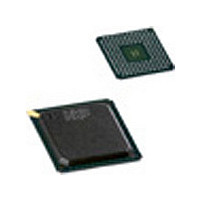
SAA7109EEB NXP Semiconductors, SAA7109EEB Datasheet - Page 124

SAA7109EEB
Manufacturer Part Number
SAA7109EEB
Description
Manufacturer
NXP Semiconductors
Datasheet
1.SAA7109EEB.pdf
(202 pages)
Specifications of SAA7109EEB
Lead Free Status / Rohs Status
Supplier Unconfirmed
- Current page: 124 of 202
- Download datasheet (984Kb)
Philips Semiconductors
18.1.1
Table 67 I
Table 68 I
Table 69 I
Table 70 I
Table 71 I
Table 72 Explanations of Tables 67 to 71
Notes
1. X is the read/write control bit; X = logic 0 is order to write; X = logic 1 is order to read.
2. If more than 1 byte of DATA is transmitted, then auto-increment of the subaddress is performed.
2004 Mar 16
S 1 0 0 0 1 0 0 0 A SUBADDRESS
S 1 0 0 0 1 0 0 0 A FEH
S 1 0 0 0 1 0 0 0 A FFH
S 1 0 0 0 1 0 0 0 A SUBADDRESS
S 1 0 0 0 1 0 0 0 A FEH
S
Sr
1 0 0 0 1 0 0 X; note 1
A
Am
SUBADDRESS; note 2
DATA
--------
P
RAM ADDRESS
PC-CODEC
I
2
C-
2
2
2
2
2
CODE
C-bus write access to control registers; see Table 72
C-bus write access to cursor bit map (subaddress FEH); see Table 72
C-bus write access to colour look-up table (subaddress FFH); see Table 72
C-bus read access to control registers; see Table 72
C-bus read access to cursor bit map or colour LUT; see Table 72
BUS FORMAT
or
FFH
START condition
repeated START condition
slave address
acknowledge generated by the slave
acknowledge generated by the master
subaddress byte
data byte
continued data bytes and acknowledges
STOP condition
start address for RAM access
A RAM ADDRESS
A RAM ADDRESS A Sr 1 0 0 0 1 0 0 1 A DATA 0 Am -------- DATA n Am P
A
RAM ADDRESS
A Sr 1 0 0 0 1 0 0 1
A DATA 0R
124
A
A
DATA 0
DATA 0
DESCRIPTION
A DATA 0
A DATA 0G
A
A
SAA7108E; SAA7109E
--------
Am
--------
A DATA 0B
--------
DATA n
DATA n
Product specification
DATA n
A --------
A
Am
A
P
P
P
P
Related parts for SAA7109EEB
Image
Part Number
Description
Manufacturer
Datasheet
Request
R

Part Number:
Description:
PC-CODEC
Manufacturer:
PHILIPS [NXP Semiconductors]
Datasheet:
Part Number:
Description:
NXP Semiconductors designed the LPC2420/2460 microcontroller around a 16-bit/32-bitARM7TDMI-S CPU core with real-time debug interfaces that include both JTAG andembedded trace
Manufacturer:
NXP Semiconductors
Datasheet:

Part Number:
Description:
NXP Semiconductors designed the LPC2458 microcontroller around a 16-bit/32-bitARM7TDMI-S CPU core with real-time debug interfaces that include both JTAG andembedded trace
Manufacturer:
NXP Semiconductors
Datasheet:
Part Number:
Description:
NXP Semiconductors designed the LPC2468 microcontroller around a 16-bit/32-bitARM7TDMI-S CPU core with real-time debug interfaces that include both JTAG andembedded trace
Manufacturer:
NXP Semiconductors
Datasheet:
Part Number:
Description:
NXP Semiconductors designed the LPC2470 microcontroller, powered by theARM7TDMI-S core, to be a highly integrated microcontroller for a wide range ofapplications that require advanced communications and high quality graphic displays
Manufacturer:
NXP Semiconductors
Datasheet:
Part Number:
Description:
NXP Semiconductors designed the LPC2478 microcontroller, powered by theARM7TDMI-S core, to be a highly integrated microcontroller for a wide range ofapplications that require advanced communications and high quality graphic displays
Manufacturer:
NXP Semiconductors
Datasheet:
Part Number:
Description:
The Philips Semiconductors XA (eXtended Architecture) family of 16-bit single-chip microcontrollers is powerful enough to easily handle the requirements of high performance embedded applications, yet inexpensive enough to compete in the market for hi
Manufacturer:
NXP Semiconductors
Datasheet:
Part Number:
Description:
The XA-S3 device is a member of Philips Semiconductors? XA(eXtended Architecture) family of high performance 16-bitsingle-chip microcontrollers
Manufacturer:
NXP Semiconductors
Datasheet:

Part Number:
Description:
The NXP BlueStreak LH75401/LH75411 family consists of two low-cost 16/32-bit System-on-Chip (SoC) devices
Manufacturer:
NXP Semiconductors
Datasheet:

Part Number:
Description:
The NXP LPC3130/3131 combine an 180 MHz ARM926EJ-S CPU core, high-speed USB2
Manufacturer:
NXP Semiconductors
Datasheet:

Part Number:
Description:
The NXP LPC3141 combine a 270 MHz ARM926EJ-S CPU core, High-speed USB 2
Manufacturer:
NXP Semiconductors

Part Number:
Description:
The NXP LPC3143 combine a 270 MHz ARM926EJ-S CPU core, High-speed USB 2
Manufacturer:
NXP Semiconductors

Part Number:
Description:
The NXP LPC3152 combines an 180 MHz ARM926EJ-S CPU core, High-speed USB 2
Manufacturer:
NXP Semiconductors

Part Number:
Description:
The NXP LPC3154 combines an 180 MHz ARM926EJ-S CPU core, High-speed USB 2
Manufacturer:
NXP Semiconductors


