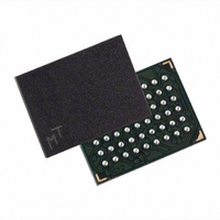
MT45W8MW16BGX-708 WT TR Micron Technology Inc, MT45W8MW16BGX-708 WT TR Datasheet - Page 15

MT45W8MW16BGX-708 WT TR
Manufacturer Part Number
MT45W8MW16BGX-708 WT TR
Description
IC PSRAM 128MBIT 70NS 54VFBGA
Manufacturer
Micron Technology Inc
Datasheet
1.MT45W8MW16BGX-708_WT_TR.pdf
(64 pages)
Specifications of MT45W8MW16BGX-708 WT TR
Format - Memory
RAM
Memory Type
PSRAM (Page)
Memory Size
128M (8Mx16)
Speed
70ns
Interface
Parallel
Voltage - Supply
1.7 V ~ 1.95 V
Operating Temperature
-30°C ~ 85°C
Package / Case
54-VFBGA
Lead Free Status / RoHS Status
Lead free / RoHS Compliant
Other names
557-1010-2
Low-Power Operation
Standby Mode Operation
reduced to the level necessary to perform the DRAM
refresh operation. Standby operation occurs when CE#
is HIGH.
completion of a READ or WRITE operation, or when
the address and control inputs remain static for an
extended period of time. This mode will continue until
a change occurs to the address or control inputs.
Temperature Compensated Refresh
adequate refresh at different temperatures. This Cellular-
RAM device includes an on-chip temperature sensor that
automatically adjusts the refresh rate according to the
operating temperature. The device continually adjusts
the refresh rate to match that temperature.
Partial Array Refresh
tion to a portion of the total memory array. This fea-
ture enables the device to reduce standby current by
refreshing only that part of the memory array required
by the host system. The refresh options are full array,
one-half array, one-quarter array, one-eighth array, or
none of the array. The mapping of these partitions can
start at either the beginning or the end of the address
map (see Table 8 on page 27). READ and WRITE opera-
tions to address ranges receiving refresh will not be
affected. Data stored in addresses not receiving refresh
will become corrupted. When re-enabling additional
portions of the array, the new portions are available
immediately upon writing to the RCR.
Deep Power-Down Operation
refresh-related activity. This mode is used if the system
does not require the storage provided by the Cellular-
RAM device. Any stored data will become corrupted
when DPD is enabled. When refresh activity has been
re-enabled, the CellularRAM device will require 150µs
to perform an initialization procedure before normal
09005aef80ec6f79 pdf/09005aef80ec6f65 zip
Burst CellularRAM 1.5_128Mb__2.fm - Rev. D 2/05 EN
During standby, the device current consumption is
The device will enter a reduced power state upon
Temperature compensated refresh (TCR) allows for
Partial array refresh (PAR) restricts refresh opera-
Deep power-down (DPD) operation disables all
ASYNC/PAGE/BURST CellularRAM 1.5 MEMORY
15
operations can resume. During this 150µs period, the
current consumption will be higher than the specified
standby levels, but considerably lower than the active
current specification.
CRE or the software access sequence; DPD starts when
CE# goes HIGH. DPD is disabled the next time CE#
goes LOW and stays LOW for at least 10µs.
Registers
the device operation. The bus configuration register
(BCR) defines how the CellularRAM interacts with the
system memory bus and is nearly identical to its coun-
terpart on burst mode Flash devices. The refresh config-
uration register (RCR) is used to control how refresh is
performed on the DRAM array. These registers are
automatically loaded with default settings during
power-up, and can be updated any time the devices
are operating in a standby state.
facturer, CellularRAM generation, and the specific
device configuration. The DIDR is read-only.
Access Using CRE
chronous or an asynchronous operation when the
control register enable (CRE) input is HIGH (see Fig-
ures 12 through 15 on pages 16 through 18). When CRE
is LOW, a READ or WRITE operation will access the
memory array. The configuration register values are
written via addresses A[22:0]. In an asynchronous
WRITE, the values are latched into the configuration
register on the rising edge of ADV#, CE#, or WE#,
whichever occurs first; LB# and UB# are “Don’t Care.”
The BCR is accessed when A[19:18] are 10b; the RCR is
accessed when A[19:18] are 00b. The DIDR is read
when A[19:18] are 01b. For reads, address inputs other
than A[19:18] are “Don’t Care,” and register bits 15:0
are output on DQ[15:0]. Immediately after performing
a configuration register READ or WRITE operation,
reading the memory array is highly recommended.
DPD can be enabled by writing to the RCR using
Two user-accessible configuration registers define
A DIDR provides information on the device manu-
The registers can be accessed using either a syn-
Micron Technology, Inc., reserves the right to change products or specifications without notice.
©2004 Micron Technology, Inc. All rights reserved.
8 MEG x 16


