DK86064-2 Fujitsu Semiconductor America Inc, DK86064-2 Datasheet - Page 21
DK86064-2
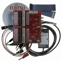
Manufacturer Part Number
DK86064-2
Description
KIT DEB DUAL 14BIT DAC MB86064
Manufacturer
Fujitsu Semiconductor America Inc
Specifications of DK86064-2
Number Of Dac's
2
Number Of Bits
14
Outputs And Type
1, Differential
Sampling Rate (per Second)
1G
Data Interface
Serial
Dac Type
Current
Voltage Supply Source
Analog and Digital
Operating Temperature
-40°C ~ 85°C
Utilized Ic / Part
MB86064
For Use With
865-1111 - DAC DK FPGA ADAPTER BOARD865-1012 - KIT DEV DUAL 14BIT MB86064 SMA
Lead Free Status / RoHS Status
Lead free / RoHS Compliant
Other names
865-1010


October 2005 Version 1.2
FME/MS/DAC80/DS/4972
MB86064 Dual 14-bit 1GSa/s DAC
The data multiplexers are controlled by the WMM Registers, WMM [EVEN/ODD] MUX CTRL. Setting
of these registers is referred to in the following two sections.
Copyright © 2004-2005 Fujitsu Microelectronics Europe GmbH
Disclaimer : The contents of this document are subject to change without notice. Customers are advised to consult with FUJITSU sales representatives before
Table 12: Waveform Memory Module Register: WMM [EVEN/ODD] MUX CTRL [0x11/0x21]
ODD] MUX CTRL
SYSTEM MISC
WMM [EVEN/
ordering.The information and circuit diagrams in this document are presented “as is”, no license is granted by implication or otherwise.
(bit)
(bit)
To use any of the Waveform Memory Module modes it is necessary to first enable the
module’s clock through register SYSTEM MISC, bit en_wmm_clk (see Table 13).
0
1
2
3
4
5
6
7
1
Table 13: DAC Core Register: SYSTEM MISC [0x1C4] (Part 3 of 3)
mux_a_ctrl[0]
mux_a_ctrl[1]
mux_a_ctrl[2]
mux_a_ctrl[3]
mux_b_ctrl[0]
mux_b_ctrl[1]
mux_b_ctrl[2]
mux_b_ctrl[3]
en_wmm_clk
Label
Label
Mux 0 control bit
0 = Data from LVDS input port A (default)
1 = Data from Mux 1
Mux 1 control bit
0 = Data from LVDS input port B (default)
1 = Data from Mux 2
Mux 2 control bit (1). See also mux_a_ctrl[3] setting.
0 = Data from RAM A - 16K points mode (default)
1 = not used
Mux 2 control bit (2)
0 = mux_a_ctrl[2] operates as normal (default)
1 = When mux_a_ctrl[2] = 0, RAM B is used instead of RAM A
Mux 0 control bit
0 = Data from LVDS input port B (default)
1 = Data from Mux 1
Mux 1 control bit
0 = Data from LVDS input port A (default)
1 = Data from Mux 2
Mux 2 control bit (1). See also mux_b_ctrl[3] setting.
0 = Data from RAM B - 16k points mode (default)
1 = not used
Mux 2 control bit (2)
0 = mux_b_ctrl[2] operates as normal (default)
1 = When mux_b_ctrl[2] = 0, RAM A is used instead of RAM B
Waveform Memory Module clock control
0 = Enabled, 1 = Disabled (default)
Function
Function
Production
Page 21 of 52
Related parts for DK86064-2
Image
Part Number
Description
Manufacturer
Datasheet
Request
R

Part Number:
Description:
IC POWER SUPPLY MONITOR 8SOP
Manufacturer:
Fujitsu Semiconductor America Inc
Datasheet:
Part Number:
Description:
IC POWER SUPPLY MONITOR 8SOP
Manufacturer:
Fujitsu Semiconductor America Inc
Datasheet:

Part Number:
Description:
IC MCU 60K FLASH 2KB RAM 52LQFP
Manufacturer:
Fujitsu Semiconductor America Inc
Datasheet:

Part Number:
Description:
IC MCU 32BIT 256KB FLASH 120LQFP
Manufacturer:
Fujitsu Semiconductor America Inc
Datasheet:
Part Number:
Description:
IC CTLR TOUCH SENSOR 12CH 30SSOP
Manufacturer:
Fujitsu Semiconductor America Inc
Datasheet:

Part Number:
Description:
IC CTLR TOUCH SENSOR 12CH 40QFN
Manufacturer:
Fujitsu Semiconductor America Inc
Datasheet:
Part Number:
Description:
SYNTHESIZER PLL DUAL INP 20SSOP
Manufacturer:
Fujitsu Semiconductor America Inc
Datasheet:

Part Number:
Description:
SYNTHESZR PLL 1.1GHZ DUAL 16SSOP
Manufacturer:
Fujitsu Semiconductor America Inc
Datasheet:

Part Number:
Description:
IC SSCG EMI RED 8-SOIC
Manufacturer:
Fujitsu Semiconductor America Inc
Datasheet:

Part Number:
Description:
IC SSCG EMI RED 8-TSSOP
Manufacturer:
Fujitsu Semiconductor America Inc
Datasheet:

Part Number:
Description:
IC SSCG EMI RED 8-SOP
Manufacturer:
Fujitsu Semiconductor America Inc
Datasheet:

Part Number:
Description:
SYNTHESIZER PLL 2.5GHZ 16SSOP
Manufacturer:
Fujitsu Semiconductor America Inc
Datasheet:
Part Number:
Description:
SYNTHESIZER PLL 1.2GHZ 16SSOP
Manufacturer:
Fujitsu Semiconductor America Inc
Datasheet:

Part Number:
Description:
SYNTHESIZER PLL 2.5GHZ 16BCC
Manufacturer:
Fujitsu Semiconductor America Inc
Datasheet:

Part Number:
Description:
IC SSCG EMI RED 8-SOP
Manufacturer:
Fujitsu Semiconductor America Inc
Datasheet: