DK86064-2 Fujitsu Semiconductor America Inc, DK86064-2 Datasheet - Page 3
DK86064-2
Manufacturer Part Number
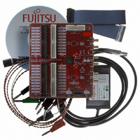
DK86064-2
Description
KIT DEB DUAL 14BIT DAC MB86064
Manufacturer
Fujitsu Semiconductor America Inc
Specifications of DK86064-2
Number Of Dac's
2
Number Of Bits
14
Outputs And Type
1, Differential
Sampling Rate (per Second)
1G
Data Interface
Serial
Dac Type
Current
Voltage Supply Source
Analog and Digital
Operating Temperature
-40°C ~ 85°C
Utilized Ic / Part
MB86064
For Use With
865-1111 - DAC DK FPGA ADAPTER BOARD865-1012 - KIT DEV DUAL 14BIT MB86064 SMA
Lead Free Status / RoHS Status
Lead free / RoHS Compliant
Other names
865-1010


October 2005 Version 1.2
FME/MS/DAC80/DS/4972
MB86064 Dual 14-bit 1GSa/s DAC
6
7
Appendix A Default Register Settings . . . . . . . . . . . . . . . . . . . . . . . . . . . . 50
Copyright © 2004-2005 Fujitsu Microelectronics Europe GmbH
Disclaimer : The contents of this document are subject to change without notice. Customers are advised to consult with FUJITSU sales representatives before
5.4 Ordering Information . . . . . . . . . . . . . . . . . . . . . . . . . . . . . . . . . . . . 39
Application Notes . . . . . . . . . . . . . . . . . . . . . . . . . . . . . . . . . . . . . . . . . 40
6.1 PCB Power & Ground Plane Splits and Decoupling . . . . . . . . . . . . 40
6.2 Input Clock Interfacing . . . . . . . . . . . . . . . . . . . . . . . . . . . . . . . . . . 42
6.3 Clock Duty Cycle Optimisation . . . . . . . . . . . . . . . . . . . . . . . . . . . . 43
6.4 Analog Output Interfacing . . . . . . . . . . . . . . . . . . . . . . . . . . . . . . . . 44
6.5 Example Setup Register Settings . . . . . . . . . . . . . . . . . . . . . . . . . . 46
6.6 Technical Support . . . . . . . . . . . . . . . . . . . . . . . . . . . . . . . . . . . . . . 47
Development Kit . . . . . . . . . . . . . . . . . . . . . . . . . . . . . . . . . . . . . . . . . . 48
7.1 Using DKUSB-1 in Target Applications . . . . . . . . . . . . . . . . . . . . . . 49
ordering.The information and circuit diagrams in this document are presented “as is”, no license is granted by implication or otherwise.
6.4.1
6.4.2
6.5.1
6.5.2
6.5.3
6.5.4
A.1
A.2
Transformer Coupled Output Circuit. . . . . . . . . . . . . . . . . . 44
Direct Interface to Quadrature Modulator . . . . . . . . . . . . . . 45
Dual DAC, LVDS data, Clock Outputs enabled . . . . . . . . . 46
Single DAC, LVDS data port A, driving DAC A . . . . . . . . . 46
Multiplexed LVDS data into DAC A (A=EVEN, B=ODD) . . 46
Waveform Memory Module, Different A & B Waveforms . . 46
DAC Core Registers. . . . . . . . . . . . . . . . . . . . . . . . . . . . 50
Waveform Memory Module Registers . . . . . . . . . . . . . . 51
This device contains circuitry to protect the inputs against damage due to high static voltages or electric fields.
However, it is advised that normal precautions be taken to avoid application of any voltage higher than maximum
rated voltages to this high impedance circuit.
without detection. Ensure proper ESD procedures are followed when handling this
High electrostatic charges can accumulate in the human body and discharge
ELECTROSTATIC DISCHARGE SENSITIVE DEVICE
Production
CAUTION
device.
Page 3 of 52
Related parts for DK86064-2
Image
Part Number
Description
Manufacturer
Datasheet
Request
R

Part Number:
Description:
IC POWER SUPPLY MONITOR 8SOP
Manufacturer:
Fujitsu Semiconductor America Inc
Datasheet:
Part Number:
Description:
IC POWER SUPPLY MONITOR 8SOP
Manufacturer:
Fujitsu Semiconductor America Inc
Datasheet:

Part Number:
Description:
IC MCU 60K FLASH 2KB RAM 52LQFP
Manufacturer:
Fujitsu Semiconductor America Inc
Datasheet:

Part Number:
Description:
IC MCU 32BIT 256KB FLASH 120LQFP
Manufacturer:
Fujitsu Semiconductor America Inc
Datasheet:
Part Number:
Description:
IC CTLR TOUCH SENSOR 12CH 30SSOP
Manufacturer:
Fujitsu Semiconductor America Inc
Datasheet:

Part Number:
Description:
IC CTLR TOUCH SENSOR 12CH 40QFN
Manufacturer:
Fujitsu Semiconductor America Inc
Datasheet:
Part Number:
Description:
SYNTHESIZER PLL DUAL INP 20SSOP
Manufacturer:
Fujitsu Semiconductor America Inc
Datasheet:

Part Number:
Description:
SYNTHESZR PLL 1.1GHZ DUAL 16SSOP
Manufacturer:
Fujitsu Semiconductor America Inc
Datasheet:

Part Number:
Description:
IC SSCG EMI RED 8-SOIC
Manufacturer:
Fujitsu Semiconductor America Inc
Datasheet:

Part Number:
Description:
IC SSCG EMI RED 8-TSSOP
Manufacturer:
Fujitsu Semiconductor America Inc
Datasheet:

Part Number:
Description:
IC SSCG EMI RED 8-SOP
Manufacturer:
Fujitsu Semiconductor America Inc
Datasheet:

Part Number:
Description:
SYNTHESIZER PLL 2.5GHZ 16SSOP
Manufacturer:
Fujitsu Semiconductor America Inc
Datasheet:
Part Number:
Description:
SYNTHESIZER PLL 1.2GHZ 16SSOP
Manufacturer:
Fujitsu Semiconductor America Inc
Datasheet:

Part Number:
Description:
SYNTHESIZER PLL 2.5GHZ 16BCC
Manufacturer:
Fujitsu Semiconductor America Inc
Datasheet:

Part Number:
Description:
IC SSCG EMI RED 8-SOP
Manufacturer:
Fujitsu Semiconductor America Inc
Datasheet: