DK86064-2 Fujitsu Semiconductor America Inc, DK86064-2 Datasheet - Page 4
DK86064-2
Manufacturer Part Number
DK86064-2
Description
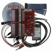
KIT DEB DUAL 14BIT DAC MB86064
Manufacturer
Fujitsu Semiconductor America Inc
Specifications of DK86064-2
Number Of Dac's
2
Number Of Bits
14
Outputs And Type
1, Differential
Sampling Rate (per Second)
1G
Data Interface
Serial
Dac Type
Current
Voltage Supply Source
Analog and Digital
Operating Temperature
-40°C ~ 85°C
Utilized Ic / Part
MB86064
For Use With
865-1111 - DAC DK FPGA ADAPTER BOARD865-1012 - KIT DEV DUAL 14BIT MB86064 SMA
Lead Free Status / RoHS Status
Lead free / RoHS Compliant
Other names
865-1010


1
The MB86064 is a high performance Dual 14-bit 1GSa/s DAC. In addition to two DAC cores the
device features a host of features designed to help both system integration and operation. A
functional block diagram is shown in Figure 1.
The device features a number of proprietary performance enhancement features. For example,
analog performance at high frequencies is enhanced by novel current switch and switch driver
designs which provide constant data-independent switching delay, reducing jitter and distortion.
Each DAC core can be regarded as two interleaved DACs running at half rate. The main reason for
adopting this approach is that the switch driver inherently includes a multiplex function through its two
input ports. Compared to a conventional switch driver this allows twice as long to acquire and convert,
though because the two paths share current sources they match exactly at low frequencies. In terms
of input data, this approach allows easy interfacing to DDR data generating devices.
Also integrated into the device is a comprehensive Waveform Memory Module (WMM). Waveforms
can be downloaded, via the serial control interface, to drive the DAC cores in the absence of a
suitable external data generator.
Page 4 of 52
Disclaimer : The contents of this document are subject to change without notice. Customers are advised to consult with FUJITSU sales representatives before
Loop clock output
Control Interface
Port A data input
Port B data input
Loop clock input
RF Clock input
1.8V LVCMOS
e.g. 500MHz
14-bit LVDS
14-bit LVDS
Functional Description
ordering.The information and circuit diagrams in this document are presented “as is”, no license is granted by implication or otherwise.
LVDS
LVDS
4-wire Serial Control Interface
Figure 1 MB86064 Functional Block Diagram
Production
Waveform
Waveform
(16K Points)
(16K Points)
Memory
Memory
Waveform
Waveform
(16K Points)
(16K Points)
Memory
Memory
A
B
A
B
Copyright © 2004-2005 Fujitsu Microelectronics Europe GmbH
MB86064 Dual 14-bit 1GSa/s DAC
1, 2, 4, 8
1, 2, 4, 8
DAC A
DAC B
October 2005 Version 1.2
EFBGA-120
(14-bit)
(14-bit)
Double-Edge
(1GSa/s)
clocked
FME/MS/DAC80/DS/4972
Clock output 1
LVDS
Clock output 2
LVDS
Analog output A
Analog output B
Related parts for DK86064-2
Image
Part Number
Description
Manufacturer
Datasheet
Request
R

Part Number:
Description:
IC POWER SUPPLY MONITOR 8SOP
Manufacturer:
Fujitsu Semiconductor America Inc
Datasheet:
Part Number:
Description:
IC POWER SUPPLY MONITOR 8SOP
Manufacturer:
Fujitsu Semiconductor America Inc
Datasheet:

Part Number:
Description:
IC MCU 60K FLASH 2KB RAM 52LQFP
Manufacturer:
Fujitsu Semiconductor America Inc
Datasheet:

Part Number:
Description:
IC MCU 32BIT 256KB FLASH 120LQFP
Manufacturer:
Fujitsu Semiconductor America Inc
Datasheet:
Part Number:
Description:
IC CTLR TOUCH SENSOR 12CH 30SSOP
Manufacturer:
Fujitsu Semiconductor America Inc
Datasheet:

Part Number:
Description:
IC CTLR TOUCH SENSOR 12CH 40QFN
Manufacturer:
Fujitsu Semiconductor America Inc
Datasheet:
Part Number:
Description:
SYNTHESIZER PLL DUAL INP 20SSOP
Manufacturer:
Fujitsu Semiconductor America Inc
Datasheet:

Part Number:
Description:
SYNTHESZR PLL 1.1GHZ DUAL 16SSOP
Manufacturer:
Fujitsu Semiconductor America Inc
Datasheet:

Part Number:
Description:
IC SSCG EMI RED 8-SOIC
Manufacturer:
Fujitsu Semiconductor America Inc
Datasheet:

Part Number:
Description:
IC SSCG EMI RED 8-TSSOP
Manufacturer:
Fujitsu Semiconductor America Inc
Datasheet:

Part Number:
Description:
IC SSCG EMI RED 8-SOP
Manufacturer:
Fujitsu Semiconductor America Inc
Datasheet:

Part Number:
Description:
SYNTHESIZER PLL 2.5GHZ 16SSOP
Manufacturer:
Fujitsu Semiconductor America Inc
Datasheet:
Part Number:
Description:
SYNTHESIZER PLL 1.2GHZ 16SSOP
Manufacturer:
Fujitsu Semiconductor America Inc
Datasheet:

Part Number:
Description:
SYNTHESIZER PLL 2.5GHZ 16BCC
Manufacturer:
Fujitsu Semiconductor America Inc
Datasheet:

Part Number:
Description:
IC SSCG EMI RED 8-SOP
Manufacturer:
Fujitsu Semiconductor America Inc
Datasheet: