DK86064-2 Fujitsu Semiconductor America Inc, DK86064-2 Datasheet - Page 43
DK86064-2
Manufacturer Part Number
DK86064-2
Description
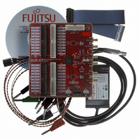
KIT DEB DUAL 14BIT DAC MB86064
Manufacturer
Fujitsu Semiconductor America Inc
Specifications of DK86064-2
Number Of Dac's
2
Number Of Bits
14
Outputs And Type
1, Differential
Sampling Rate (per Second)
1G
Data Interface
Serial
Dac Type
Current
Voltage Supply Source
Analog and Digital
Operating Temperature
-40°C ~ 85°C
Utilized Ic / Part
MB86064
For Use With
865-1111 - DAC DK FPGA ADAPTER BOARD865-1012 - KIT DEV DUAL 14BIT MB86064 SMA
Lead Free Status / RoHS Status
Lead free / RoHS Compliant
Other names
865-1010


October 2005 Version 1.2
FME/MS/DAC80/DS/4972
MB86064 Dual 14-bit 1GSa/s DAC
6.3
Earlier sections of this data sheet document that the DAC core is clocked on both rising and falling
edges of the input clock, and that a characteristic of this architecture is suppressed images of the
generated signal relating to Fclk. Any duty cycle error in the input clock will exacerbate the Fclk-Fsig
image. This can be minimised by using a filtered, sinusoidal clock and if necessary trimming the
differential DC offset.
Applications using a square wave clock are unlikely to achieve the 50:50 duty cycle necessary to
deliver best wide-band spurious performance. Measurements and calculations show that for an
output at 3/8Fdac a duty cycle error of 1% (49:51) gives 32dBc rejection. In cases where maximal
suppression of the Fclk-Fsig image is required it is recommended to either filter the clock or
implement a tuned circuit as part of the clock routing.
A band-pass filter can be used but a low-pass response allows for some variation in clock frequency
to be accommodated. A key target of the filter is to suppress the second harmonic by 40dB. This will
reduce the duty cycle error by approximately 100 times, or in other words to a negligible level. For
most applications a third order L-C filter should meet these requirements. It is important to ensure
that the resultant clock amplitude meets the required specification otherwise phase noise will
increase due to reduced slew rate.
An alternative is to construct a tuned circuit by linking CLK to CLKB with two 50 delay lines, one at
the clock source and the other at the DAC. The delay time required is equivalent to one half of a clock
period. The delay line links will need to be AC coupled from the clock source if a DC short is not
supported. Similarly, AC coupling with appropriate biassing, prior to the DAC input, would be
necessary where trimming of the differential DC offset is required. This approach has also
demonstrated a reduction in duty cycle error by approximately 100 times. The two delay lines can be
implemented in the PCB tracking. The length of tracking required depends on the PCB signal
propagation speed. For example, a delay of 1.35ns would be used in system operating at a clock
frequency of about 370MHz, and would be realised with a PCB track length of about 27cm, assuming
5ns/m propagation speed on the PCB. Tracking the delay would be by zig-zagging backwards and
forwards on a spare inner layer. The two delay lines must be separated by PCB tracks sufficiently
long that a clock edge finishes exiting the first delay line before entering the second, i.e. td > tr, or
spacing > 10cm for tr=0.5ns.
Copyright © 2004-2005 Fujitsu Microelectronics Europe GmbH
Disclaimer : The contents of this document are subject to change without notice. Customers are advised to consult with FUJITSU sales representatives before
Square Wave
Clock Source
Clock Duty Cycle Optimisation
ordering.The information and circuit diagrams in this document are presented “as is”, no license is granted by implication or otherwise.
Figure 21 Clock Duty Cycle Optimisation using Delay Line Links
1
Line Link
st
Delay
Production
2
Line Link
nd
Delay
MB86064
Clock Input
Page 43 of 52
Related parts for DK86064-2
Image
Part Number
Description
Manufacturer
Datasheet
Request
R

Part Number:
Description:
IC POWER SUPPLY MONITOR 8SOP
Manufacturer:
Fujitsu Semiconductor America Inc
Datasheet:
Part Number:
Description:
IC POWER SUPPLY MONITOR 8SOP
Manufacturer:
Fujitsu Semiconductor America Inc
Datasheet:

Part Number:
Description:
IC MCU 60K FLASH 2KB RAM 52LQFP
Manufacturer:
Fujitsu Semiconductor America Inc
Datasheet:

Part Number:
Description:
IC MCU 32BIT 256KB FLASH 120LQFP
Manufacturer:
Fujitsu Semiconductor America Inc
Datasheet:
Part Number:
Description:
IC CTLR TOUCH SENSOR 12CH 30SSOP
Manufacturer:
Fujitsu Semiconductor America Inc
Datasheet:

Part Number:
Description:
IC CTLR TOUCH SENSOR 12CH 40QFN
Manufacturer:
Fujitsu Semiconductor America Inc
Datasheet:
Part Number:
Description:
SYNTHESIZER PLL DUAL INP 20SSOP
Manufacturer:
Fujitsu Semiconductor America Inc
Datasheet:

Part Number:
Description:
SYNTHESZR PLL 1.1GHZ DUAL 16SSOP
Manufacturer:
Fujitsu Semiconductor America Inc
Datasheet:

Part Number:
Description:
IC SSCG EMI RED 8-SOIC
Manufacturer:
Fujitsu Semiconductor America Inc
Datasheet:

Part Number:
Description:
IC SSCG EMI RED 8-TSSOP
Manufacturer:
Fujitsu Semiconductor America Inc
Datasheet:

Part Number:
Description:
IC SSCG EMI RED 8-SOP
Manufacturer:
Fujitsu Semiconductor America Inc
Datasheet:

Part Number:
Description:
SYNTHESIZER PLL 2.5GHZ 16SSOP
Manufacturer:
Fujitsu Semiconductor America Inc
Datasheet:
Part Number:
Description:
SYNTHESIZER PLL 1.2GHZ 16SSOP
Manufacturer:
Fujitsu Semiconductor America Inc
Datasheet:

Part Number:
Description:
SYNTHESIZER PLL 2.5GHZ 16BCC
Manufacturer:
Fujitsu Semiconductor America Inc
Datasheet:

Part Number:
Description:
IC SSCG EMI RED 8-SOP
Manufacturer:
Fujitsu Semiconductor America Inc
Datasheet: