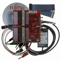
DK86064-2 Fujitsu Semiconductor America Inc, DK86064-2 Datasheet - Page 27

DK86064-2
Manufacturer Part Number
DK86064-2
Description
KIT DEB DUAL 14BIT DAC MB86064
Manufacturer
Fujitsu Semiconductor America Inc
Specifications of DK86064-2
Number Of Dac's
2
Number Of Bits
14
Outputs And Type
1, Differential
Sampling Rate (per Second)
1G
Data Interface
Serial
Dac Type
Current
Voltage Supply Source
Analog and Digital
Operating Temperature
-40°C ~ 85°C
Utilized Ic / Part
MB86064
For Use With
865-1111 - DAC DK FPGA ADAPTER BOARD865-1012 - KIT DEV DUAL 14BIT MB86064 SMA
Lead Free Status / RoHS Status
Lead free / RoHS Compliant
Other names
865-1010
October 2005 Version 1.2
FME/MS/DAC80/DS/4972
MB86064 Dual 14-bit 1GSa/s DAC
Once the RAM Access Controller returns to the idle state, after a successful write sequence, data
transfer starts automatically. However, until the other RAM element is programmed and the RAMs
are synchronised, the output sequence will be corrupt.
• repeat the above sequence for the ODD RAM element.
The order in which the EVEN/ODD RAMs are programmed is not important.
Once all of the required RAMs have been programmed, the RAM Access Controllers need to be set
to ‘run’ and synchronised by a software reset, see Section 3.3. Finally, ensure that all ODD, EVEN
and the WMM/LVDS data multiplexers are set appropriately. A worked example is given in section
6.5.4
3.3
The Waveform Memory Module may be reset through a software reset function. This is activated
through register BIST [EVEN/ODD] CONFIG bit swrst.
Copyright © 2004-2005 Fujitsu Microelectronics Europe GmbH
Disclaimer : The contents of this document are subject to change without notice. Customers are advised to consult with FUJITSU sales representatives before
ODD] CONFIG
WMM [EVEN/
Table 19: WMM Register: WMM [EVEN/ODD] CONFIG [0x10/0x20] (Part 2 of 2)
Software Reset
ordering.The information and circuit diagrams in this document are presented “as is”, no license is granted by implication or otherwise.
(bit)
Programming the WMM / LVDS data source multiplexer bit ‘data_direct’ last will prevent
incomplete and unsynchronised data reaching the DAC before it is required.
Two writes to ‘swrst’ are required to produce a software reset; first setting (1) and then
clearing (0). Writing to both ODD and EVEN registers (0x10 or 0x20) is not necessary as
either register will synchronise all memories.
0
Label
swrst
Software reset control bit
0 = Normal operation (default) , 1 = Software Reset
Function
Production
Page 27 of 52


