DK86064-2 Fujitsu Semiconductor America Inc, DK86064-2 Datasheet - Page 24
DK86064-2
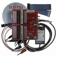
Manufacturer Part Number
DK86064-2
Description
KIT DEB DUAL 14BIT DAC MB86064
Manufacturer
Fujitsu Semiconductor America Inc
Specifications of DK86064-2
Number Of Dac's
2
Number Of Bits
14
Outputs And Type
1, Differential
Sampling Rate (per Second)
1G
Data Interface
Serial
Dac Type
Current
Voltage Supply Source
Analog and Digital
Operating Temperature
-40°C ~ 85°C
Utilized Ic / Part
MB86064
For Use With
865-1111 - DAC DK FPGA ADAPTER BOARD865-1012 - KIT DEV DUAL 14BIT MB86064 SMA
Lead Free Status / RoHS Status
Lead free / RoHS Compliant
Other names
865-1010


ODD and EVEN RAM elements within the module allow data to be routed to the ODD and EVEN
phase DAC core data latches, similar to when data is input via the LVDS data interface and double
edge clocking is used. As an example, to route data from RAM A to DAC A, and RAM B to DAC B,
• set register WMM [EVEN/ODD] MUX CTRL bits mux_a_ctrl[1] & [0] and mux_b_ctrl[1] & [0]. Both
To swap these data paths,
• set register WMM [EVEN/ODD] MUX CTRL bits mux_a_ctrl[3] and mux_b_ctrl[3]. Both the EVEN
3.2.1 Waveform Memory Access via the Serial Interface
To access the waveform memories the RAM Access Controllers must first be configured. The RAM
Access Controllers are configured through registers WMM [EVEN/ODD] RAM CTRL. See Table 17.
Page 24 of 52
Disclaimer : The contents of this document are subject to change without notice. Customers are advised to consult with FUJITSU sales representatives before
Table 17: Waveform Memory Module Registers: WMM [EVEN/ODD] RAM CTRL [0x12/0x22]
the EVEN and ODD registers should be set the same. All other bits should be set to their default
value.
and ODD registers should be set the same.
ODD] RAM CTRL
WMM [EVEN/
ordering.The information and circuit diagrams in this document are presented “as is”, no license is granted by implication or otherwise.
(bits)
[21:11]
[10:0]
When programming the WMM on-chip memories ensure that the Clock Input (f
greater than 16 times the serial interface clock frequency (f
22
23
24
25
prog_sel(1)
prog_sel(2)
prog_burst
prog_addr
prog_start
prog_rw
Label
Production
RAM access start address
RAM access burst size
Access burst size should be programmed as ((No. of points/8) - 1)
A value of zero indicates a single word access
RAM serial interface access mode
0 = Read mode (default)
1 = Write mode
RAM write select (1). Dependent on prog_sel(2) setting
0 = Write data to RAM A (default)
1 = Write data to RAM B
RAM write select (2)
0 = prog_sel(1) operates as normal (default)
1 = Writes the same data to both RAM A and RAM B
RAM Access Controller control
0 = Cycle through vector address range (default)
1 = Program RAMs
This bit is self clearing
Copyright © 2004-2005 Fujitsu Microelectronics Europe GmbH
MB86064 Dual 14-bit 1GSa/s DAC
Function
sclk
October 2005 Version 1.2
) for correct operation.
FME/MS/DAC80/DS/4972
Clk
) is
Related parts for DK86064-2
Image
Part Number
Description
Manufacturer
Datasheet
Request
R

Part Number:
Description:
IC POWER SUPPLY MONITOR 8SOP
Manufacturer:
Fujitsu Semiconductor America Inc
Datasheet:
Part Number:
Description:
IC POWER SUPPLY MONITOR 8SOP
Manufacturer:
Fujitsu Semiconductor America Inc
Datasheet:

Part Number:
Description:
IC MCU 60K FLASH 2KB RAM 52LQFP
Manufacturer:
Fujitsu Semiconductor America Inc
Datasheet:

Part Number:
Description:
IC MCU 32BIT 256KB FLASH 120LQFP
Manufacturer:
Fujitsu Semiconductor America Inc
Datasheet:
Part Number:
Description:
IC CTLR TOUCH SENSOR 12CH 30SSOP
Manufacturer:
Fujitsu Semiconductor America Inc
Datasheet:

Part Number:
Description:
IC CTLR TOUCH SENSOR 12CH 40QFN
Manufacturer:
Fujitsu Semiconductor America Inc
Datasheet:
Part Number:
Description:
SYNTHESIZER PLL DUAL INP 20SSOP
Manufacturer:
Fujitsu Semiconductor America Inc
Datasheet:

Part Number:
Description:
SYNTHESZR PLL 1.1GHZ DUAL 16SSOP
Manufacturer:
Fujitsu Semiconductor America Inc
Datasheet:

Part Number:
Description:
IC SSCG EMI RED 8-SOIC
Manufacturer:
Fujitsu Semiconductor America Inc
Datasheet:

Part Number:
Description:
IC SSCG EMI RED 8-TSSOP
Manufacturer:
Fujitsu Semiconductor America Inc
Datasheet:

Part Number:
Description:
IC SSCG EMI RED 8-SOP
Manufacturer:
Fujitsu Semiconductor America Inc
Datasheet:

Part Number:
Description:
SYNTHESIZER PLL 2.5GHZ 16SSOP
Manufacturer:
Fujitsu Semiconductor America Inc
Datasheet:
Part Number:
Description:
SYNTHESIZER PLL 1.2GHZ 16SSOP
Manufacturer:
Fujitsu Semiconductor America Inc
Datasheet:

Part Number:
Description:
SYNTHESIZER PLL 2.5GHZ 16BCC
Manufacturer:
Fujitsu Semiconductor America Inc
Datasheet:

Part Number:
Description:
IC SSCG EMI RED 8-SOP
Manufacturer:
Fujitsu Semiconductor America Inc
Datasheet: