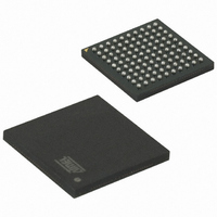
AT91SAM7X256B-CU Atmel, AT91SAM7X256B-CU Datasheet - Page 141

AT91SAM7X256B-CU
Manufacturer Part Number
AT91SAM7X256B-CU
Description
IC MCU 256KB FLASH 100TFBGA
Manufacturer
Atmel
Series
AT91SAMr
Specifications of AT91SAM7X256B-CU
Core Processor
ARM7
Core Size
16/32-Bit
Speed
55MHz
Connectivity
CAN, Ethernet, I²C, SPI, SSC, UART/USART, USB
Peripherals
Brown-out Detect/Reset, DMA, POR, PWM, WDT
Number Of I /o
62
Program Memory Size
256KB (256K x 8)
Program Memory Type
FLASH
Ram Size
64K x 8
Voltage - Supply (vcc/vdd)
1.65 V ~ 1.95 V
Data Converters
A/D 8x10b
Oscillator Type
Internal
Operating Temperature
-40°C ~ 85°C
Package / Case
100-TFBGA
Processor Series
91S
Core
ARM7TDMI
Data Bus Width
32 bit
Data Ram Size
64 KB
Interface Type
CAN, Ethernet, SPI, I2S, TWI, USART, USB
Maximum Clock Frequency
55 MHz
Number Of Programmable I/os
62
Number Of Timers
3
Operating Supply Voltage
3.3 V
Maximum Operating Temperature
+ 85 C
Mounting Style
SMD/SMT
Minimum Operating Temperature
- 40 C
Operating Temperature Range
- 40 C to + 85 C
Package
100TFBGA
Device Core
ARM7TDMI
Family Name
91S
Maximum Speed
55 MHz
On-chip Adc
8-chx10-bit
Lead Free Status / RoHS Status
Lead free / RoHS Compliant
Eeprom Size
-
Lead Free Status / Rohs Status
Details
Available stocks
Company
Part Number
Manufacturer
Quantity
Price
- Current page: 141 of 687
- Download datasheet (11Mb)
22. Peripheral DMA Controller (PDC)
22.1
22.2
6120H–ATARM–17-Feb-09
Overview
Block Diagram
The Peripheral DMA Controller (PDC) transfers data between on-chip serial peripherals such as
the UART, USART, SSC, SPI, MCI and the on- and off-chip memories. Using the Peripheral
DMA Controller avoids processor intervention and removes the processor interrupt-handling
overhead. This significantly reduces the number of clock cycles required for a data transfer and,
as a result, improves the performance of the microcontroller and makes it more power efficient.
The PDC channels are implemented in pairs, each pair being dedicated to a particular periph-
eral. One channel in the pair is dedicated to the receiving channel and one to the transmitting
channel of each UART, USART, SSC and SPI.
The user interface of a PDC channel is integrated in the memory space of each peripheral. It
contains:
The peripheral triggers PDC transfers using transmit and receive signals. When the pro-
grammed data is transferred, an end of transfer interrupt is generated by the corresponding
peripheral.
Figure 22-1. Block Diagram
• A 32-bit memory pointer register
• A 16-bit transfer count register
• A 32-bit register for next memory pointer
• A 16-bit register for next transfer count
Peripheral
Control
THR
RHR
AT91SAM7X512/256/128 Preliminary
Status & Control
PDC Channel 0
PDC Channel 1
Peripheral DMA Controller
Control
Controller
Memory
141
Related parts for AT91SAM7X256B-CU
Image
Part Number
Description
Manufacturer
Datasheet
Request
R

Part Number:
Description:
KIT EVAL FOR AT91SAM7X256/128
Manufacturer:
Atmel
Datasheet:

Part Number:
Description:
MCU, MPU & DSP Development Tools KICKSTART KIT ATMEL AT91SAM7X
Manufacturer:
IAR Systems

Part Number:
Description:
MCU ARM9 64K SRAM 144-LFBGA
Manufacturer:
Atmel
Datasheet:

Part Number:
Description:
IC ARM7 MCU FLASH 256K 100LQFP
Manufacturer:
Atmel
Datasheet:

Part Number:
Description:
IC ARM9 MPU 217-LFBGA
Manufacturer:
Atmel
Datasheet:

Part Number:
Description:
MCU ARM9 ULTRA LOW PWR 217-LFBGA
Manufacturer:
Atmel
Datasheet:

Part Number:
Description:
MCU ARM9 324-TFBGA
Manufacturer:
Atmel
Datasheet:

Part Number:
Description:
IC MCU ARM9 SAMPLING 217CBGA
Manufacturer:
Atmel
Datasheet:

Part Number:
Description:
IC ARM9 MCU 217-LFBGA
Manufacturer:
Atmel
Datasheet:

Part Number:
Description:
IC ARM9 MCU 208-PQFP
Manufacturer:
Atmel
Datasheet:

Part Number:
Description:
MCU ARM 512K HS FLASH 100-LQFP
Manufacturer:
Atmel
Datasheet:

Part Number:
Description:
MCU ARM 512K HS FLASH 100-TFBGA
Manufacturer:
Atmel
Datasheet:

Part Number:
Description:
IC ARM9 MCU 200 MHZ 324-TFBGA
Manufacturer:
Atmel
Datasheet:

Part Number:
Description:
IC ARM MCU 16BIT 128K 256BGA
Manufacturer:
Atmel
Datasheet:

Part Number:
Description:
IC ARM7 MCU 32BIT 128K 64LQFP
Manufacturer:
Atmel
Datasheet:


