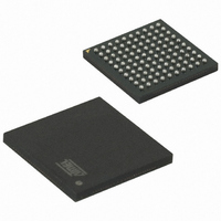
AT91SAM7X256B-CU Atmel, AT91SAM7X256B-CU Datasheet - Page 37

AT91SAM7X256B-CU
Manufacturer Part Number
AT91SAM7X256B-CU
Description
IC MCU 256KB FLASH 100TFBGA
Manufacturer
Atmel
Series
AT91SAMr
Specifications of AT91SAM7X256B-CU
Core Processor
ARM7
Core Size
16/32-Bit
Speed
55MHz
Connectivity
CAN, Ethernet, I²C, SPI, SSC, UART/USART, USB
Peripherals
Brown-out Detect/Reset, DMA, POR, PWM, WDT
Number Of I /o
62
Program Memory Size
256KB (256K x 8)
Program Memory Type
FLASH
Ram Size
64K x 8
Voltage - Supply (vcc/vdd)
1.65 V ~ 1.95 V
Data Converters
A/D 8x10b
Oscillator Type
Internal
Operating Temperature
-40°C ~ 85°C
Package / Case
100-TFBGA
Processor Series
91S
Core
ARM7TDMI
Data Bus Width
32 bit
Data Ram Size
64 KB
Interface Type
CAN, Ethernet, SPI, I2S, TWI, USART, USB
Maximum Clock Frequency
55 MHz
Number Of Programmable I/os
62
Number Of Timers
3
Operating Supply Voltage
3.3 V
Maximum Operating Temperature
+ 85 C
Mounting Style
SMD/SMT
Minimum Operating Temperature
- 40 C
Operating Temperature Range
- 40 C to + 85 C
Package
100TFBGA
Device Core
ARM7TDMI
Family Name
91S
Maximum Speed
55 MHz
On-chip Adc
8-chx10-bit
Lead Free Status / RoHS Status
Lead free / RoHS Compliant
Eeprom Size
-
Lead Free Status / Rohs Status
Details
Available stocks
Company
Part Number
Manufacturer
Quantity
Price
- Current page: 37 of 687
- Download datasheet (11Mb)
10.12 Pulse Width Modulation Controller
10.13 USB Device Port
6120H–ATARM–17-Feb-09
Table 10-4.
TC Clock input
TIMER_CLOCK1
TIMER_CLOCK2
TIMER_CLOCK3
TIMER_CLOCK4
TIMER_CLOCK5
• Each channel is user-configurable and contains:
• Five internal clock inputs, as defined in
• Four channels, one 16-bit counter per channel
• Common clock generator, providing thirteen different clocks
• Independent channel programming
• USB V2.0 full-speed compliant,12 Mbits per second
• Embedded USB V2.0 full-speed transceiver
• Embedded 1352-byte dual-port RAM for endpoints
• Six endpoints
– Pulse generation
– Delay timing
– Pulse Width Modulation
– Up/down capabilities
– Three external clock inputs
– Two multi-purpose input/output signals
– Two global registers that act on all three TC channels
– One Modulo n counter providing eleven clocks
– Two independent linear dividers working on modulo n counter outputs
– Independent enable/disable commands
– Independent clock selection
– Independent period and duty cycle, with double buffering
– Programmable selection of the output waveform polarity
– Programmable center or left aligned output waveform
– Endpoint 0: 8 bytes
– Endpoint 1 and 2: 64 bytes ping-pong
– Endpoint 3: 64 bytes
– Endpoint 4 and 5: 256 bytes ping-pong
– Ping-pong Mode (two memory banks) for bulk endpoints
Timer Counter Clocks Assignment
AT91SAM7X512/256/128 Preliminary
Table 10-4
Clock
MCK/2
MCK/8
MCK/32
MCK/128
MCK/1024
37
Related parts for AT91SAM7X256B-CU
Image
Part Number
Description
Manufacturer
Datasheet
Request
R

Part Number:
Description:
KIT EVAL FOR AT91SAM7X256/128
Manufacturer:
Atmel
Datasheet:

Part Number:
Description:
MCU, MPU & DSP Development Tools KICKSTART KIT ATMEL AT91SAM7X
Manufacturer:
IAR Systems

Part Number:
Description:
MCU ARM9 64K SRAM 144-LFBGA
Manufacturer:
Atmel
Datasheet:

Part Number:
Description:
IC ARM7 MCU FLASH 256K 100LQFP
Manufacturer:
Atmel
Datasheet:

Part Number:
Description:
IC ARM9 MPU 217-LFBGA
Manufacturer:
Atmel
Datasheet:

Part Number:
Description:
MCU ARM9 ULTRA LOW PWR 217-LFBGA
Manufacturer:
Atmel
Datasheet:

Part Number:
Description:
MCU ARM9 324-TFBGA
Manufacturer:
Atmel
Datasheet:

Part Number:
Description:
IC MCU ARM9 SAMPLING 217CBGA
Manufacturer:
Atmel
Datasheet:

Part Number:
Description:
IC ARM9 MCU 217-LFBGA
Manufacturer:
Atmel
Datasheet:

Part Number:
Description:
IC ARM9 MCU 208-PQFP
Manufacturer:
Atmel
Datasheet:

Part Number:
Description:
MCU ARM 512K HS FLASH 100-LQFP
Manufacturer:
Atmel
Datasheet:

Part Number:
Description:
MCU ARM 512K HS FLASH 100-TFBGA
Manufacturer:
Atmel
Datasheet:

Part Number:
Description:
IC ARM9 MCU 200 MHZ 324-TFBGA
Manufacturer:
Atmel
Datasheet:

Part Number:
Description:
IC ARM MCU 16BIT 128K 256BGA
Manufacturer:
Atmel
Datasheet:

Part Number:
Description:
IC ARM7 MCU 32BIT 128K 64LQFP
Manufacturer:
Atmel
Datasheet:


