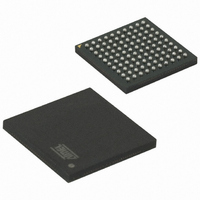
AT91SAM7X256B-CU Atmel, AT91SAM7X256B-CU Datasheet - Page 427

AT91SAM7X256B-CU
Manufacturer Part Number
AT91SAM7X256B-CU
Description
IC MCU 256KB FLASH 100TFBGA
Manufacturer
Atmel
Series
AT91SAMr
Specifications of AT91SAM7X256B-CU
Core Processor
ARM7
Core Size
16/32-Bit
Speed
55MHz
Connectivity
CAN, Ethernet, I²C, SPI, SSC, UART/USART, USB
Peripherals
Brown-out Detect/Reset, DMA, POR, PWM, WDT
Number Of I /o
62
Program Memory Size
256KB (256K x 8)
Program Memory Type
FLASH
Ram Size
64K x 8
Voltage - Supply (vcc/vdd)
1.65 V ~ 1.95 V
Data Converters
A/D 8x10b
Oscillator Type
Internal
Operating Temperature
-40°C ~ 85°C
Package / Case
100-TFBGA
Processor Series
91S
Core
ARM7TDMI
Data Bus Width
32 bit
Data Ram Size
64 KB
Interface Type
CAN, Ethernet, SPI, I2S, TWI, USART, USB
Maximum Clock Frequency
55 MHz
Number Of Programmable I/os
62
Number Of Timers
3
Operating Supply Voltage
3.3 V
Maximum Operating Temperature
+ 85 C
Mounting Style
SMD/SMT
Minimum Operating Temperature
- 40 C
Operating Temperature Range
- 40 C to + 85 C
Package
100TFBGA
Device Core
ARM7TDMI
Family Name
91S
Maximum Speed
55 MHz
On-chip Adc
8-chx10-bit
Lead Free Status / RoHS Status
Lead free / RoHS Compliant
Eeprom Size
-
Lead Free Status / Rohs Status
Details
Available stocks
Company
Part Number
Manufacturer
Quantity
Price
- Current page: 427 of 687
- Download datasheet (11Mb)
6120H–ATARM–17-Feb-09
Figure 33-4. Non Overlapped Center Aligned Waveforms
Note:
• the waveform duty cycle. This channel parameter is defined in the CDTY field of the
• the waveform polarity. At the beginning of the period, the signal can be at high or low level.
• the waveform alignment. The output waveform can be left or center aligned. Center aligned
By using a Master Clock divided by one of both DIVA or DIVB divider, the formula becomes,
respectively:
If the waveform is center aligned then the output waveform period depends on the counter
source clock and can be calculated:
By using the Master Clock (MCK) divided by an X given prescaler value
(with X being 1, 2, 4, 8, 16, 32, 64, 128, 256, 512, or 1024). The resulting period formula will
be:
By using a Master Clock divided by one of both DIVA or DIVB divider, the formula becomes,
respectively:
PWM_CDTYx register.
If the waveform is left aligned then:
If the waveform is center aligned, then:
This property is defined in the CPOL field of the PWM_CMRx register. By default the signal
starts by a low level.
waveforms can be used to generate non overlapped waveforms. This property is defined in
the CALG field of the PWM_CMRx register. The default mode is left aligned.
(
------------------------------------------ -
(
------------------------------------------ -
(
----------------------------------------------------- -
PWM0
PWM1
CRPD
2
2
duty cycle
duty cycle
×
×
X
CPRD
See
MCK
MCK
×
MCK
×
CPRD
Figure 33-5 on page 429
DIVA
×
=
DIVA
=
No overlap
)
)
(
----------------------------------------------------------------------------------------------------------- -
(
----------------------------------------------------------------------------------------------------------------------------- -
period 1
or
(
period
)
(
---------------------------------------------- -
or
CRPD
AT91SAM7X512/256/128 Preliminary
Period
(
----------------------------------------------------- -
–
2
⁄
MCK
×
×
2
⁄
CPRD
) 1
DIVAB
fchannel_x_clock
–
MCK
for a detailed description of center aligned waveforms.
period
⁄
(
×
period
)
fchannel_x_clock
DIVB
)
⁄
2
)
×
CDTY
×
CDTY
)
) )
427
Related parts for AT91SAM7X256B-CU
Image
Part Number
Description
Manufacturer
Datasheet
Request
R

Part Number:
Description:
KIT EVAL FOR AT91SAM7X256/128
Manufacturer:
Atmel
Datasheet:

Part Number:
Description:
MCU, MPU & DSP Development Tools KICKSTART KIT ATMEL AT91SAM7X
Manufacturer:
IAR Systems

Part Number:
Description:
MCU ARM9 64K SRAM 144-LFBGA
Manufacturer:
Atmel
Datasheet:

Part Number:
Description:
IC ARM7 MCU FLASH 256K 100LQFP
Manufacturer:
Atmel
Datasheet:

Part Number:
Description:
IC ARM9 MPU 217-LFBGA
Manufacturer:
Atmel
Datasheet:

Part Number:
Description:
MCU ARM9 ULTRA LOW PWR 217-LFBGA
Manufacturer:
Atmel
Datasheet:

Part Number:
Description:
MCU ARM9 324-TFBGA
Manufacturer:
Atmel
Datasheet:

Part Number:
Description:
IC MCU ARM9 SAMPLING 217CBGA
Manufacturer:
Atmel
Datasheet:

Part Number:
Description:
IC ARM9 MCU 217-LFBGA
Manufacturer:
Atmel
Datasheet:

Part Number:
Description:
IC ARM9 MCU 208-PQFP
Manufacturer:
Atmel
Datasheet:

Part Number:
Description:
MCU ARM 512K HS FLASH 100-LQFP
Manufacturer:
Atmel
Datasheet:

Part Number:
Description:
MCU ARM 512K HS FLASH 100-TFBGA
Manufacturer:
Atmel
Datasheet:

Part Number:
Description:
IC ARM9 MCU 200 MHZ 324-TFBGA
Manufacturer:
Atmel
Datasheet:

Part Number:
Description:
IC ARM MCU 16BIT 128K 256BGA
Manufacturer:
Atmel
Datasheet:

Part Number:
Description:
IC ARM7 MCU 32BIT 128K 64LQFP
Manufacturer:
Atmel
Datasheet:


