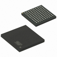
AT91SAM7X256B-CU Atmel, AT91SAM7X256B-CU Datasheet - Page 656

AT91SAM7X256B-CU
Manufacturer Part Number
AT91SAM7X256B-CU
Description
IC MCU 256KB FLASH 100TFBGA
Manufacturer
Atmel
Series
AT91SAMr
Specifications of AT91SAM7X256B-CU
Core Processor
ARM7
Core Size
16/32-Bit
Speed
55MHz
Connectivity
CAN, Ethernet, I²C, SPI, SSC, UART/USART, USB
Peripherals
Brown-out Detect/Reset, DMA, POR, PWM, WDT
Number Of I /o
62
Program Memory Size
256KB (256K x 8)
Program Memory Type
FLASH
Ram Size
64K x 8
Voltage - Supply (vcc/vdd)
1.65 V ~ 1.95 V
Data Converters
A/D 8x10b
Oscillator Type
Internal
Operating Temperature
-40°C ~ 85°C
Package / Case
100-TFBGA
Processor Series
91S
Core
ARM7TDMI
Data Bus Width
32 bit
Data Ram Size
64 KB
Interface Type
CAN, Ethernet, SPI, I2S, TWI, USART, USB
Maximum Clock Frequency
55 MHz
Number Of Programmable I/os
62
Number Of Timers
3
Operating Supply Voltage
3.3 V
Maximum Operating Temperature
+ 85 C
Mounting Style
SMD/SMT
Minimum Operating Temperature
- 40 C
Operating Temperature Range
- 40 C to + 85 C
Package
100TFBGA
Device Core
ARM7TDMI
Family Name
91S
Maximum Speed
55 MHz
On-chip Adc
8-chx10-bit
Lead Free Status / RoHS Status
Lead free / RoHS Compliant
Eeprom Size
-
Lead Free Status / Rohs Status
Details
Available stocks
Company
Part Number
Manufacturer
Quantity
Price
- Current page: 656 of 687
- Download datasheet (11Mb)
41.3.9
41.3.9.1
41.3.9.2
41.3.9.3
656
AT91SAM7X512/256/128 Preliminary
Synchronous Serial Controller (SSC)
SSC: Periodic Transmission Limitations in Master Mode
SSC: Transmitter Limitations in Slave Mode
SSC: Transmitter Limitations in Slave Mode
If the Least Significant Bit is sent first (MSBF = 0), the first TAG during the frame synchro is not
sent.
None.
If TK is programmed as output and TF is programmed as input, it is impossible to emit data
when the start of edge (rising or falling) of synchro has a Start Delay equal to zero.
None.
If TK is programmed as an input and TF is programmed as an output and requested to be set to
low/high during data emission, the Frame Synchro signal is generated one bit clock period after
the data start and one data bit is lost. This problem does not exist when generating a periodic
synchro.
The data need to be delayed for one bit clock period with an external assembly. In the following
schematic, TD, TK and NRST are AT91SAM7X signals, TXD is the delayed data to connect to
the device.
Problem Fix/Workaround
Problem Fix/Workaround
Problem Fix/Workaround
6120H–ATARM–17-Feb-09
Related parts for AT91SAM7X256B-CU
Image
Part Number
Description
Manufacturer
Datasheet
Request
R

Part Number:
Description:
KIT EVAL FOR AT91SAM7X256/128
Manufacturer:
Atmel
Datasheet:

Part Number:
Description:
MCU, MPU & DSP Development Tools KICKSTART KIT ATMEL AT91SAM7X
Manufacturer:
IAR Systems

Part Number:
Description:
MCU ARM9 64K SRAM 144-LFBGA
Manufacturer:
Atmel
Datasheet:

Part Number:
Description:
IC ARM7 MCU FLASH 256K 100LQFP
Manufacturer:
Atmel
Datasheet:

Part Number:
Description:
IC ARM9 MPU 217-LFBGA
Manufacturer:
Atmel
Datasheet:

Part Number:
Description:
MCU ARM9 ULTRA LOW PWR 217-LFBGA
Manufacturer:
Atmel
Datasheet:

Part Number:
Description:
MCU ARM9 324-TFBGA
Manufacturer:
Atmel
Datasheet:

Part Number:
Description:
IC MCU ARM9 SAMPLING 217CBGA
Manufacturer:
Atmel
Datasheet:

Part Number:
Description:
IC ARM9 MCU 217-LFBGA
Manufacturer:
Atmel
Datasheet:

Part Number:
Description:
IC ARM9 MCU 208-PQFP
Manufacturer:
Atmel
Datasheet:

Part Number:
Description:
MCU ARM 512K HS FLASH 100-LQFP
Manufacturer:
Atmel
Datasheet:

Part Number:
Description:
MCU ARM 512K HS FLASH 100-TFBGA
Manufacturer:
Atmel
Datasheet:

Part Number:
Description:
IC ARM9 MCU 200 MHZ 324-TFBGA
Manufacturer:
Atmel
Datasheet:

Part Number:
Description:
IC ARM MCU 16BIT 128K 256BGA
Manufacturer:
Atmel
Datasheet:

Part Number:
Description:
IC ARM7 MCU 32BIT 128K 64LQFP
Manufacturer:
Atmel
Datasheet:


