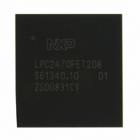
LPC2470FET208,551 NXP Semiconductors, LPC2470FET208,551 Datasheet - Page 302

LPC2470FET208,551
Manufacturer Part Number
LPC2470FET208,551
Description
IC ARM7 MCU LCD 208-TFBGA
Manufacturer
NXP Semiconductors
Series
LPC2400r
Datasheets
1.OM11077.pdf
(792 pages)
2.LPC2470FET208551.pdf
(89 pages)
3.LPC2470FET208551.pdf
(91 pages)
Specifications of LPC2470FET208,551
Package / Case
208-TFBGA
Core Processor
ARM7
Core Size
16/32-Bit
Speed
72MHz
Connectivity
CAN, EBI/EMI, Ethernet, I²C, Microwire, MMC, SPI, SSI, SSP, UART/USART, USB OTG
Peripherals
Brown-out Detect/Reset, DMA, I²S, LCD, POR, PWM, WDT
Number Of I /o
160
Program Memory Type
ROMless
Ram Size
98K x 8
Voltage - Supply (vcc/vdd)
3 V ~ 3.6 V
Data Converters
A/D 8x10b; D/A 1x10b
Oscillator Type
Internal
Operating Temperature
-40°C ~ 85°C
Processor Series
LPC24
Core
ARM7TDMI-S
Data Bus Width
16 bit, 32 bit
Data Ram Size
98 KB
Interface Type
CAN/I2C/I2S/SPI/SSP/UART/USB
Maximum Clock Frequency
72 MHz
Number Of Programmable I/os
160
Number Of Timers
4
Maximum Operating Temperature
+ 85 C
Mounting Style
SMD/SMT
3rd Party Development Tools
MDK-ARM, RL-ARM, ULINK2, MCB2470U
Minimum Operating Temperature
- 40 C
On-chip Adc
8-ch x 10-bit
On-chip Dac
1-ch x 10-bit
Package
208TFBGA
Device Core
ARM7TDMI-S
Family Name
LPC2000
Maximum Speed
72 MHz
Operating Supply Voltage
3.3 V
Lead Free Status / RoHS Status
Lead free / RoHS Compliant
Eeprom Size
-
Program Memory Size
-
Lead Free Status / Rohs Status
Lead free / RoHS Compliant
Other names
568-4362
935284071551
LPC2470FET208-S
935284071551
LPC2470FET208-S
Available stocks
Company
Part Number
Manufacturer
Quantity
Price
Company:
Part Number:
LPC2470FET208,551
Manufacturer:
Exar
Quantity:
92
Company:
Part Number:
LPC2470FET208,551
Manufacturer:
NXP Semiconductors
Quantity:
10 000
- Current page: 302 of 792
- Download datasheet (5Mb)
NXP Semiconductors
UM10237_4
User manual
6.12 LCD power-up and power-down sequence
The LCD controller requires the following power-up sequence to be performed:
1. When power is applied, the following signals are held LOW:
2. When LCD power is stabilized, a 1 is written to the LcdEn bit in the LCD_CTRL register.
This enables the following signals into their active states:
The LCDV[23:0] signals remain in an inactive state.
3. When the signals in step 2 have stabilized, the contrast voltage (not controlled or
supplied by the LCD controller) is applied to the LCD panel.
4. If required, a software or hardware timer can be used to provide the minimum display
specific delay time between application of the control signals and power to the panel
display. On completion of the time interval, power is applied to the panel by writing a 1 to
the LcdPwr bit within the LCD_CTRL register that, in turn, sets the LCDPWR signal high
and enables the LCDV[23:0] signals into their active states. The LCDPWR signal is
intended to be used to gate the power to the LCD panel.
The power-down sequence is the reverse of the above four steps and must be strictly
followed, this time, writing the respective register bits with 0.
Figure 12–40
•
•
•
•
•
•
•
•
•
•
•
LCDLP
LCDDCLK
LCDFP
LCDENAB/ LCDM
LCDVD[23:0]
LCDLE
LCDLP
LCDDCLK
LCDFP
LCDENAB/ LCDM
LCDLE
shows the power-up and power-down sequences.
Rev. 04 — 26 August 2009
Chapter 12: LPC24XX LCD controller
UM10237
© NXP B.V. 2009. All rights reserved.
302 of 792
Related parts for LPC2470FET208,551
Image
Part Number
Description
Manufacturer
Datasheet
Request
R
Part Number:
Description:
NXP Semiconductors designed the LPC2470 microcontroller, powered by theARM7TDMI-S core, to be a highly integrated microcontroller for a wide range ofapplications that require advanced communications and high quality graphic displays
Manufacturer:
NXP Semiconductors
Datasheet:
Part Number:
Description:
NXP Semiconductors designed the LPC2420/2460 microcontroller around a 16-bit/32-bitARM7TDMI-S CPU core with real-time debug interfaces that include both JTAG andembedded trace
Manufacturer:
NXP Semiconductors
Datasheet:

Part Number:
Description:
NXP Semiconductors designed the LPC2458 microcontroller around a 16-bit/32-bitARM7TDMI-S CPU core with real-time debug interfaces that include both JTAG andembedded trace
Manufacturer:
NXP Semiconductors
Datasheet:
Part Number:
Description:
NXP Semiconductors designed the LPC2468 microcontroller around a 16-bit/32-bitARM7TDMI-S CPU core with real-time debug interfaces that include both JTAG andembedded trace
Manufacturer:
NXP Semiconductors
Datasheet:
Part Number:
Description:
NXP Semiconductors designed the LPC2478 microcontroller, powered by theARM7TDMI-S core, to be a highly integrated microcontroller for a wide range ofapplications that require advanced communications and high quality graphic displays
Manufacturer:
NXP Semiconductors
Datasheet:
Part Number:
Description:
The Philips Semiconductors XA (eXtended Architecture) family of 16-bit single-chip microcontrollers is powerful enough to easily handle the requirements of high performance embedded applications, yet inexpensive enough to compete in the market for hi
Manufacturer:
NXP Semiconductors
Datasheet:
Part Number:
Description:
The XA-S3 device is a member of Philips Semiconductors? XA(eXtended Architecture) family of high performance 16-bitsingle-chip microcontrollers
Manufacturer:
NXP Semiconductors
Datasheet:

Part Number:
Description:
The NXP BlueStreak LH75401/LH75411 family consists of two low-cost 16/32-bit System-on-Chip (SoC) devices
Manufacturer:
NXP Semiconductors
Datasheet:

Part Number:
Description:
The NXP LPC3130/3131 combine an 180 MHz ARM926EJ-S CPU core, high-speed USB2
Manufacturer:
NXP Semiconductors
Datasheet:

Part Number:
Description:
The NXP LPC3141 combine a 270 MHz ARM926EJ-S CPU core, High-speed USB 2
Manufacturer:
NXP Semiconductors

Part Number:
Description:
The NXP LPC3143 combine a 270 MHz ARM926EJ-S CPU core, High-speed USB 2
Manufacturer:
NXP Semiconductors

Part Number:
Description:
The NXP LPC3152 combines an 180 MHz ARM926EJ-S CPU core, High-speed USB 2
Manufacturer:
NXP Semiconductors

Part Number:
Description:
The NXP LPC3154 combines an 180 MHz ARM926EJ-S CPU core, High-speed USB 2
Manufacturer:
NXP Semiconductors

Part Number:
Description:
Standard level N-channel enhancement mode Field-Effect Transistor (FET) in a plastic package using NXP High-Performance Automotive (HPA) TrenchMOS technology
Manufacturer:
NXP Semiconductors
Datasheet:


