MC9S08GT32CFDE Freescale Semiconductor, MC9S08GT32CFDE Datasheet - Page 118
MC9S08GT32CFDE
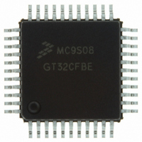
Manufacturer Part Number
MC9S08GT32CFDE
Description
IC MCU 32K FLASH 20MHZ 48-QFN
Manufacturer
Freescale Semiconductor
Series
HCS08r
Specifications of MC9S08GT32CFDE
Core Processor
HCS08
Core Size
8-Bit
Speed
40MHz
Connectivity
I²C, SCI, SPI
Peripherals
LVD, POR, PWM, WDT
Number Of I /o
39
Program Memory Size
32KB (32K x 8)
Program Memory Type
FLASH
Ram Size
2K x 8
Voltage - Supply (vcc/vdd)
1.8 V ~ 3.6 V
Data Converters
A/D 8x10b
Oscillator Type
Internal
Operating Temperature
-40°C ~ 85°C
Package / Case
48-QFN
Controller Family/series
HCS08
No. Of I/o's
39
Ram Memory Size
2KB
Cpu Speed
40MHz
No. Of Timers
2
Rohs Compliant
Yes
For Use With
M68DEMO908GB60E - BOARD DEMO MC9S08GB60M68EVB908GB60E - BOARD EVAL FOR MC9S08GB60
Lead Free Status / RoHS Status
Lead free / RoHS Compliant
Eeprom Size
-


Internal Clock Generator (ICG) Module
7.5.1
RANGE — Frequency Range Select
REFS — External Reference Select
CLKS — Clock Mode Select
The CLKS bits are writable at any time, unless the first write after a reset was CLKS = 0X, the CLKS bits
cannot be written to 1X until after the next reset (because the EXTAL pin was not reserved).
118
1. This bit is reserved for Freescale Semiconductor internal use only. Any write operations to this register should write
The RANGE bit controls the oscillator, reference divider, and FLL loop prescaler multiplication factor
(P). It selects one of two reference frequency ranges for the ICG. The RANGE bit is write-once after
a reset. The RANGE bit only has an effect in FLL engaged external and FLL bypassed external modes.
The REFS bit controls the external reference clock source for ICGERCLK. The REFS bit is write-once
after a reset.
The CLKS bits control the clock mode according to
requested, it will not be selected until ERCS = 1. If the ICG enters off mode, the CLKS bits will remain
unchanged.Writes to the CLKS bits will not take effect if a previous write is not complete.
a 0 to this bit.
1 = Oscillator configured for high frequency range. FLL loop prescale factor P is 1.
0 = Oscillator configured for low frequency range. FLL loop prescale factor P is 64.
1 = Oscillator using crystal or resonator requested.
0 = External clock requested.
ICG Control Register 1 (ICGC1)
Reset:
Read:
Write:
Bit 7
0
0
CLKS[1:0]
Figure 7-12. ICG Control Register 1 (ICGC1)
00
01
10
11
= Unimplemented or Reserved
RANGE
MC9S08GB/GT Data Sheet, Rev. 2.3
Figure 7-13. CLKS Clock Select
6
1
REFS
FLL bypassed, external reference
FLL engaged, external reference
FLL engaged, internal reference
5
0
Self-clocked
Clock Mode
Figure
4
0
CLKS
7-13. If FLL bypassed external is
3
0
OSCSTEN
2
1
Freescale Semiconductor
0
1
(1)
0
Bit 0
0
0
Related parts for MC9S08GT32CFDE
Image
Part Number
Description
Manufacturer
Datasheet
Request
R

Part Number:
Description:
Manufacturer:
Freescale Semiconductor, Inc
Datasheet:
Part Number:
Description:
Manufacturer:
Freescale Semiconductor, Inc
Datasheet:
Part Number:
Description:
Manufacturer:
Freescale Semiconductor, Inc
Datasheet:
Part Number:
Description:
Manufacturer:
Freescale Semiconductor, Inc
Datasheet:
Part Number:
Description:
Manufacturer:
Freescale Semiconductor, Inc
Datasheet:
Part Number:
Description:
Manufacturer:
Freescale Semiconductor, Inc
Datasheet:
Part Number:
Description:
Manufacturer:
Freescale Semiconductor, Inc
Datasheet:
Part Number:
Description:
Manufacturer:
Freescale Semiconductor, Inc
Datasheet:
Part Number:
Description:
Manufacturer:
Freescale Semiconductor, Inc
Datasheet:
Part Number:
Description:
Manufacturer:
Freescale Semiconductor, Inc
Datasheet:
Part Number:
Description:
Manufacturer:
Freescale Semiconductor, Inc
Datasheet:
Part Number:
Description:
Manufacturer:
Freescale Semiconductor, Inc
Datasheet:
Part Number:
Description:
Manufacturer:
Freescale Semiconductor, Inc
Datasheet:
Part Number:
Description:
Manufacturer:
Freescale Semiconductor, Inc
Datasheet:
Part Number:
Description:
Manufacturer:
Freescale Semiconductor, Inc
Datasheet: