MC9S08GT32CFDE Freescale Semiconductor, MC9S08GT32CFDE Datasheet - Page 71
MC9S08GT32CFDE
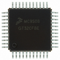
Manufacturer Part Number
MC9S08GT32CFDE
Description
IC MCU 32K FLASH 20MHZ 48-QFN
Manufacturer
Freescale Semiconductor
Series
HCS08r
Specifications of MC9S08GT32CFDE
Core Processor
HCS08
Core Size
8-Bit
Speed
40MHz
Connectivity
I²C, SCI, SPI
Peripherals
LVD, POR, PWM, WDT
Number Of I /o
39
Program Memory Size
32KB (32K x 8)
Program Memory Type
FLASH
Ram Size
2K x 8
Voltage - Supply (vcc/vdd)
1.8 V ~ 3.6 V
Data Converters
A/D 8x10b
Oscillator Type
Internal
Operating Temperature
-40°C ~ 85°C
Package / Case
48-QFN
Controller Family/series
HCS08
No. Of I/o's
39
Ram Memory Size
2KB
Cpu Speed
40MHz
No. Of Timers
2
Rohs Compliant
Yes
For Use With
M68DEMO908GB60E - BOARD DEMO MC9S08GB60M68EVB908GB60E - BOARD EVAL FOR MC9S08GB60
Lead Free Status / RoHS Status
Lead free / RoHS Compliant
Eeprom Size
-


LVD — Low Voltage Detect
5.8.3
This register contains a single write-only control bit. A serial background command such as
WRITE_BYTE must be used to write to SBDFR. Attempts to write this register from a user program are
ignored. Reads always return $00.
BDFR — Background Debug Force Reset
5.8.4
This register may be read at any time. Bits 3 and 2 are unimplemented and always read 0. This is a
write-once register so only the first write after reset is honored. Any subsequent attempt to write to SOPT
(intentionally or unintentionally) is ignored to avoid accidental changes to these sensitive settings. SOPT
should be written during the user’s reset initialization program to set the desired controls even if the desired
settings are the same as the reset settings.
Freescale Semiconductor
If the LVD reset is enabled (LVDE = LVDRE = 1) and the supply drops below the LVD trip voltage,
an LVD reset occurs. The LVD function is disabled when the MCU enters stop. To maintain LVD
operation in stop, the LVDSE bit must be set.
A serial background mode command such as WRITE_BYTE allows an external debug host to force a
target system reset. Writing 1 to this bit forces an MCU reset. This bit cannot be written from a user
program.
1
BDFR is writable only through serial background debug commands, not from user programs.
1 = Reset caused by LVD trip or POR.
0 = Reset not caused by LVD trip or POR.
System Background Debug Force Reset Register (SBDFR)
System Options Register (SOPT)
Figure 5-4. System Background Debug Force Reset Register (SBDFR)
Reset:
Reset:
Read:
Write:
Read:
Write:
COPE
Bit 7
Bit 7
Figure 5-5. System Options Register (SOPT)
0
0
1
= Unimplemented or Reserved
= Unimplemented or Reserved
MC9S08GB/GT Data Sheet, Rev. 2.3
COPT
6
0
0
6
1
STOPE
5
0
0
5
0
Reset, Interrupt, and System Control Registers and Control Bits
4
0
0
4
1
3
0
0
3
0
0
2
0
0
2
0
0
BKGDPE
1
0
0
1
1
BDFR
Bit 0
Bit 0
0
0
1
1
71
Related parts for MC9S08GT32CFDE
Image
Part Number
Description
Manufacturer
Datasheet
Request
R

Part Number:
Description:
Manufacturer:
Freescale Semiconductor, Inc
Datasheet:
Part Number:
Description:
Manufacturer:
Freescale Semiconductor, Inc
Datasheet:
Part Number:
Description:
Manufacturer:
Freescale Semiconductor, Inc
Datasheet:
Part Number:
Description:
Manufacturer:
Freescale Semiconductor, Inc
Datasheet:
Part Number:
Description:
Manufacturer:
Freescale Semiconductor, Inc
Datasheet:
Part Number:
Description:
Manufacturer:
Freescale Semiconductor, Inc
Datasheet:
Part Number:
Description:
Manufacturer:
Freescale Semiconductor, Inc
Datasheet:
Part Number:
Description:
Manufacturer:
Freescale Semiconductor, Inc
Datasheet:
Part Number:
Description:
Manufacturer:
Freescale Semiconductor, Inc
Datasheet:
Part Number:
Description:
Manufacturer:
Freescale Semiconductor, Inc
Datasheet:
Part Number:
Description:
Manufacturer:
Freescale Semiconductor, Inc
Datasheet:
Part Number:
Description:
Manufacturer:
Freescale Semiconductor, Inc
Datasheet:
Part Number:
Description:
Manufacturer:
Freescale Semiconductor, Inc
Datasheet:
Part Number:
Description:
Manufacturer:
Freescale Semiconductor, Inc
Datasheet:
Part Number:
Description:
Manufacturer:
Freescale Semiconductor, Inc
Datasheet: