MC9S08GT32CFDE Freescale Semiconductor, MC9S08GT32CFDE Datasheet - Page 230
MC9S08GT32CFDE
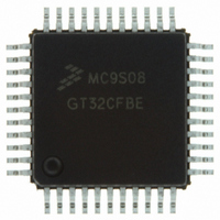
Manufacturer Part Number
MC9S08GT32CFDE
Description
IC MCU 32K FLASH 20MHZ 48-QFN
Manufacturer
Freescale Semiconductor
Series
HCS08r
Specifications of MC9S08GT32CFDE
Core Processor
HCS08
Core Size
8-Bit
Speed
40MHz
Connectivity
I²C, SCI, SPI
Peripherals
LVD, POR, PWM, WDT
Number Of I /o
39
Program Memory Size
32KB (32K x 8)
Program Memory Type
FLASH
Ram Size
2K x 8
Voltage - Supply (vcc/vdd)
1.8 V ~ 3.6 V
Data Converters
A/D 8x10b
Oscillator Type
Internal
Operating Temperature
-40°C ~ 85°C
Package / Case
48-QFN
Controller Family/series
HCS08
No. Of I/o's
39
Ram Memory Size
2KB
Cpu Speed
40MHz
No. Of Timers
2
Rohs Compliant
Yes
For Use With
M68DEMO908GB60E - BOARD DEMO MC9S08GB60M68EVB908GB60E - BOARD EVAL FOR MC9S08GB60
Lead Free Status / RoHS Status
Lead free / RoHS Compliant
Eeprom Size
-


Analog-to-Digital Converter (ATD) Module
14.6.1
Writes to the ATD control register will abort the current conversion, but will not start a new conversion.
ATDPU — ATD Power Up
DJM — Data Justification Mode
230
ATD1RH
ATD1RH
This bit provides program on/off control over the ATD, reducing power consumption when the ATD
is not being used. When cleared, the ATDPU bit aborts any conversion in progress.
This bit determines how the 10-bit conversion result data maps onto the ATD result register bits. When
RES8 is set, bit DJM has no effect and the 8-bit result is always located in ATD1RH.
For left-justified mode, result data bits 9–2 map onto bits 7–0 of ATD1RH, result data bits 1 and 0 map
onto ATD1RL bits 7 and 6, where bit 7 of ATD1RH is the most significant bit (MSB).
For right-justified mode, result data bits 9 and 8 map onto bits 1 and 0 of ATD1RH, result data bits
7–0 map onto ATD1RL bits 7–0, where bit 1 of ATD1RH is the most significant bit (MSB).
The effect of the DJM bit on the result is shown in
7
9
7
1 = ATD functionality.
0 = Disable the ATD and enter a low-power state.
1 = Result register data is right justified.
0 = Result register data is left justified.
ATD Control (ATDC)
6
6
5
5
Reset:
Read:
Write:
4
4
ATDPU
Bit 7
3
3
0
RESULT
Figure 14-5. ATD Control Register (ATD1C)
2
2
Figure 14-7. Right-Justified Mode
Figure 14-6. Left-Justified Mode
MC9S08GB/GT Data Sheet, Rev. 2.3
DJM
6
0
1
1
9
RES8
0
0
5
0
ATD1RL
ATD1RL
Table
SGN
7
7
4
0
14-3.
6
0
6
3
0
RESULT
5
5
4
4
2
0
PRS
3
3
Freescale Semiconductor
1
0
2
2
Bit 0
1
1
0
0
0
0
Related parts for MC9S08GT32CFDE
Image
Part Number
Description
Manufacturer
Datasheet
Request
R

Part Number:
Description:
Manufacturer:
Freescale Semiconductor, Inc
Datasheet:
Part Number:
Description:
Manufacturer:
Freescale Semiconductor, Inc
Datasheet:
Part Number:
Description:
Manufacturer:
Freescale Semiconductor, Inc
Datasheet:
Part Number:
Description:
Manufacturer:
Freescale Semiconductor, Inc
Datasheet:
Part Number:
Description:
Manufacturer:
Freescale Semiconductor, Inc
Datasheet:
Part Number:
Description:
Manufacturer:
Freescale Semiconductor, Inc
Datasheet:
Part Number:
Description:
Manufacturer:
Freescale Semiconductor, Inc
Datasheet:
Part Number:
Description:
Manufacturer:
Freescale Semiconductor, Inc
Datasheet:
Part Number:
Description:
Manufacturer:
Freescale Semiconductor, Inc
Datasheet:
Part Number:
Description:
Manufacturer:
Freescale Semiconductor, Inc
Datasheet:
Part Number:
Description:
Manufacturer:
Freescale Semiconductor, Inc
Datasheet:
Part Number:
Description:
Manufacturer:
Freescale Semiconductor, Inc
Datasheet:
Part Number:
Description:
Manufacturer:
Freescale Semiconductor, Inc
Datasheet:
Part Number:
Description:
Manufacturer:
Freescale Semiconductor, Inc
Datasheet:
Part Number:
Description:
Manufacturer:
Freescale Semiconductor, Inc
Datasheet: