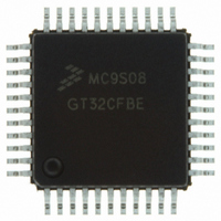
MC9S08GT32CFDE Freescale Semiconductor, MC9S08GT32CFDE Datasheet - Page 97

MC9S08GT32CFDE
Manufacturer Part Number
MC9S08GT32CFDE
Description
IC MCU 32K FLASH 20MHZ 48-QFN
Manufacturer
Freescale Semiconductor
Series
HCS08r
Specifications of MC9S08GT32CFDE
Core Processor
HCS08
Core Size
8-Bit
Speed
40MHz
Connectivity
I²C, SCI, SPI
Peripherals
LVD, POR, PWM, WDT
Number Of I /o
39
Program Memory Size
32KB (32K x 8)
Program Memory Type
FLASH
Ram Size
2K x 8
Voltage - Supply (vcc/vdd)
1.8 V ~ 3.6 V
Data Converters
A/D 8x10b
Oscillator Type
Internal
Operating Temperature
-40°C ~ 85°C
Package / Case
48-QFN
Controller Family/series
HCS08
No. Of I/o's
39
Ram Memory Size
2KB
Cpu Speed
40MHz
No. Of Timers
2
Rohs Compliant
Yes
For Use With
M68DEMO908GB60E - BOARD DEMO MC9S08GB60M68EVB908GB60E - BOARD EVAL FOR MC9S08GB60
Lead Free Status / RoHS Status
Lead free / RoHS Compliant
Eeprom Size
-
- Current page: 97 of 290
- Download datasheet (2Mb)
Chapter 7 Internal Clock Generator (ICG) Module
The MC9S08GB/GT microcontroller provides one internal clock generation (ICG) module to create the
system bus frequency. All functions described in this section are available on the MC9S08GB/GT
microcontroller. The EXTAL and XTAL pins share port G bits 2 and 1, respectively. Analog supply lines
V
the ICG may be found in
Freescale Semiconductor
DDA
ICG
and V
SSA
ICGLCLK*
ICGERCLK
FFE
* ICGLCLK is the alternate BDC clock source for the MC9S08GB/GT.
Freescale Semiconductor recommends that FLASH location $FFBE be
reserved to store a nonvolatile version of ICGTRM. This will allow
debugger and programmer vendors to perform a manual trim operation and
store the resultant ICGTRM value for users to access at a later time.
ICGOUT
are internally derived from the MCU’s V
CPU
÷
CONTROL
2
SYSTEM
LOGIC
÷
Appendix A, “Electrical
2
FIXED FREQ CLOCK (XCLK)
Figure 7-1. System Clock Distribution Diagram
RTI
BUSCLK
MC9S08GB/GT Data Sheet, Rev. 2.3
BDC
TPM1
NOTE
Characteristics.”
TPM2
DD
and V
ATD has min and max
frequency requirements.
See
and
Characteristics.
IIC1
SS
Appendix A, “Electrical
Chapter 1,
ATD1
pins. Electrical parametric data for
SCI1
“Introduction”
RAM
SCI2
FLASH has frequency
requirements for program
and erase operation.
See
Characteristics.
FLASH
Appendix A, “Electrical
SPI1
97
Related parts for MC9S08GT32CFDE
Image
Part Number
Description
Manufacturer
Datasheet
Request
R
Part Number:
Description:
Manufacturer:
Freescale Semiconductor, Inc
Datasheet:
Part Number:
Description:
Manufacturer:
Freescale Semiconductor, Inc
Datasheet:
Part Number:
Description:
Manufacturer:
Freescale Semiconductor, Inc
Datasheet:
Part Number:
Description:
Manufacturer:
Freescale Semiconductor, Inc
Datasheet:
Part Number:
Description:
Manufacturer:
Freescale Semiconductor, Inc
Datasheet:
Part Number:
Description:
Manufacturer:
Freescale Semiconductor, Inc
Datasheet:
Part Number:
Description:
Manufacturer:
Freescale Semiconductor, Inc
Datasheet:
Part Number:
Description:
Manufacturer:
Freescale Semiconductor, Inc
Datasheet:
Part Number:
Description:
Manufacturer:
Freescale Semiconductor, Inc
Datasheet:
Part Number:
Description:
Manufacturer:
Freescale Semiconductor, Inc
Datasheet:
Part Number:
Description:
Manufacturer:
Freescale Semiconductor, Inc
Datasheet:
Part Number:
Description:
Manufacturer:
Freescale Semiconductor, Inc
Datasheet:
Part Number:
Description:
Manufacturer:
Freescale Semiconductor, Inc
Datasheet:
Part Number:
Description:
Manufacturer:
Freescale Semiconductor, Inc
Datasheet:
Part Number:
Description:
Manufacturer:
Freescale Semiconductor, Inc
Datasheet:


