MC9S08GT32CFDE Freescale Semiconductor, MC9S08GT32CFDE Datasheet - Page 55
MC9S08GT32CFDE
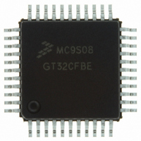
Manufacturer Part Number
MC9S08GT32CFDE
Description
IC MCU 32K FLASH 20MHZ 48-QFN
Manufacturer
Freescale Semiconductor
Series
HCS08r
Specifications of MC9S08GT32CFDE
Core Processor
HCS08
Core Size
8-Bit
Speed
40MHz
Connectivity
I²C, SCI, SPI
Peripherals
LVD, POR, PWM, WDT
Number Of I /o
39
Program Memory Size
32KB (32K x 8)
Program Memory Type
FLASH
Ram Size
2K x 8
Voltage - Supply (vcc/vdd)
1.8 V ~ 3.6 V
Data Converters
A/D 8x10b
Oscillator Type
Internal
Operating Temperature
-40°C ~ 85°C
Package / Case
48-QFN
Controller Family/series
HCS08
No. Of I/o's
39
Ram Memory Size
2KB
Cpu Speed
40MHz
No. Of Timers
2
Rohs Compliant
Yes
For Use With
M68DEMO908GB60E - BOARD DEMO MC9S08GB60M68EVB908GB60E - BOARD EVAL FOR MC9S08GB60
Lead Free Status / RoHS Status
Lead free / RoHS Compliant
Eeprom Size
-


4.6.2
During reset, the contents of the nonvolatile location NVOPT are copied from FLASH into FOPT. Bits 5
through 2 are not used and always read 0. This register may be read at any time, but writes have no meaning
or effect. To change the value in this register, erase and reprogram the NVOPT location in FLASH memory
as usual and then issue a new MCU reset.
KEYEN — Backdoor Key Mechanism Enable
FNORED — Vector Redirection Disable
Freescale Semiconductor
When this bit is 0, the backdoor key mechanism cannot be used to disengage security. The backdoor
key mechanism is accessible only from user (secured) firmware. BDM commands cannot be used to
write key comparison values that would unlock the backdoor key. For more detailed information about
the backdoor key mechanism, refer to
When this bit is 1, vector redirection is disabled.
1 = If user firmware writes an 8-byte value that matches the nonvolatile backdoor key
0 = No backdoor key access allowed.
1 = Vector redirection disabled.
0 = Vector redirection enabled.
FLASH Options Register (FOPT and NVOPT)
(NVBACKKEY through NVBACKKEY+7, in that order), security is temporarily disengaged
until the next MCU reset.
200 kHz
150 kHz
20 MHz
10 MHz
8 MHz
4 MHz
2 MHz
1 MHz
f
Bus
Reset:
Read:
Write:
(Binary)
PRDIV8
1
0
0
0
0
0
0
0
KEYEN
Bit 7
Figure 4-5. FLASH Options Register (FOPT)
Table 4-6. FLASH Clock Divider Settings
= Unimplemented or Reserved
MC9S08GB/GT Data Sheet, Rev. 2.3
DIV5:DIV0
(Decimal)
FNORED
This register is loaded from nonvolatile location NVOPT during reset.
12
49
39
19
6
9
4
0
0
Section 4.5,
0
5
192.3 kHz
200 kHz
200 kHz
200 kHz
200 kHz
200 kHz
200 kHz
150 kHz
f
FCLK
“Security.”
0
4
Program/Erase Timing Pulse
(5 µs Min, 6.7 µs Max)
0
3
5.2 µs
6.7 µs
5 µs
5 µs
5 µs
5 µs
5 µs
5 µs
0
2
FLASH Registers and Control Bits
SEC01
1
SEC00
Bit 0
55
Related parts for MC9S08GT32CFDE
Image
Part Number
Description
Manufacturer
Datasheet
Request
R

Part Number:
Description:
Manufacturer:
Freescale Semiconductor, Inc
Datasheet:
Part Number:
Description:
Manufacturer:
Freescale Semiconductor, Inc
Datasheet:
Part Number:
Description:
Manufacturer:
Freescale Semiconductor, Inc
Datasheet:
Part Number:
Description:
Manufacturer:
Freescale Semiconductor, Inc
Datasheet:
Part Number:
Description:
Manufacturer:
Freescale Semiconductor, Inc
Datasheet:
Part Number:
Description:
Manufacturer:
Freescale Semiconductor, Inc
Datasheet:
Part Number:
Description:
Manufacturer:
Freescale Semiconductor, Inc
Datasheet:
Part Number:
Description:
Manufacturer:
Freescale Semiconductor, Inc
Datasheet:
Part Number:
Description:
Manufacturer:
Freescale Semiconductor, Inc
Datasheet:
Part Number:
Description:
Manufacturer:
Freescale Semiconductor, Inc
Datasheet:
Part Number:
Description:
Manufacturer:
Freescale Semiconductor, Inc
Datasheet:
Part Number:
Description:
Manufacturer:
Freescale Semiconductor, Inc
Datasheet:
Part Number:
Description:
Manufacturer:
Freescale Semiconductor, Inc
Datasheet:
Part Number:
Description:
Manufacturer:
Freescale Semiconductor, Inc
Datasheet:
Part Number:
Description:
Manufacturer:
Freescale Semiconductor, Inc
Datasheet: