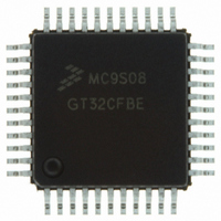
MC9S08GT32CFDE Freescale Semiconductor, MC9S08GT32CFDE Datasheet - Page 72

MC9S08GT32CFDE
Manufacturer Part Number
MC9S08GT32CFDE
Description
IC MCU 32K FLASH 20MHZ 48-QFN
Manufacturer
Freescale Semiconductor
Series
HCS08r
Specifications of MC9S08GT32CFDE
Core Processor
HCS08
Core Size
8-Bit
Speed
40MHz
Connectivity
I²C, SCI, SPI
Peripherals
LVD, POR, PWM, WDT
Number Of I /o
39
Program Memory Size
32KB (32K x 8)
Program Memory Type
FLASH
Ram Size
2K x 8
Voltage - Supply (vcc/vdd)
1.8 V ~ 3.6 V
Data Converters
A/D 8x10b
Oscillator Type
Internal
Operating Temperature
-40°C ~ 85°C
Package / Case
48-QFN
Controller Family/series
HCS08
No. Of I/o's
39
Ram Memory Size
2KB
Cpu Speed
40MHz
No. Of Timers
2
Rohs Compliant
Yes
For Use With
M68DEMO908GB60E - BOARD DEMO MC9S08GB60M68EVB908GB60E - BOARD EVAL FOR MC9S08GB60
Lead Free Status / RoHS Status
Lead free / RoHS Compliant
Eeprom Size
-
- Current page: 72 of 290
- Download datasheet (2Mb)
Chapter 5 Resets, Interrupts, and System Configuration
COPE — COP Watchdog Enable
COPT — COP Watchdog Timeout
STOPE — Stop Mode Enable
BKGDPE — Background Debug Mode Pin Enable
5.8.5
This read-only register is included so host development systems can identify the HCS08 derivative and
revision number. This allows the development software to recognize where specific memory blocks,
registers, and control bits are located in a target MCU.
REV[3:0] — Revision Number
72
This write-once bit defaults to 1 after reset.
This write-once bit defaults to 1 after reset.
This write-once bit defaults to 0 after reset, which disables stop mode. If stop mode is disabled and a
user program attempts to execute a STOP instruction, an illegal opcode reset is forced.
The BKGDPE bit enables the PTG0/BKGD/MS pin to function as BKGD/MS. When the bit is clear,
the pin will function as PTG0, which is an output-only general-purpose I/O. This pin always defaults
to BKGD/MS function after any reset.
The high-order 4 bits of address $1806 are hard coded to reflect the current mask set revision number
(0–F).
1
1 = COP watchdog timer enabled (force reset on timeout).
0 = COP watchdog timer disabled.
1 = Long timeout period selected (2
0 = Short timeout period selected (2
1 = Stop mode enabled.
0 = Stop mode disabled.
1 = BKGD pin enabled.
0 = BKGD pin disabled.
The revision number that is hard coded into these bits reflects the current silicon revision level.
System Device Identification Register (SDIDH, SDIDL)
Figure 5-6. System Device Identification Register (SDIDH, SDIDL)
Reset:
Reset:
Read:
Read:
REV3
Bit 7
ID7
0
0
1
= Unimplemented or Reserved
MC9S08GB/GT Data Sheet, Rev. 2.3
REV2
0
ID6
6
0
(1)
18
13
cycles of BUSCLK).
cycles of BUSCLK).
REV1
0
ID5
5
0
(1)
REV0
0
ID4
4
0
(1)
ID11
ID3
3
0
0
ID10
ID2
2
0
0
Freescale Semiconductor
ID9
ID1
1
0
1
Bit 0
ID8
ID0
0
0
Related parts for MC9S08GT32CFDE
Image
Part Number
Description
Manufacturer
Datasheet
Request
R
Part Number:
Description:
Manufacturer:
Freescale Semiconductor, Inc
Datasheet:
Part Number:
Description:
Manufacturer:
Freescale Semiconductor, Inc
Datasheet:
Part Number:
Description:
Manufacturer:
Freescale Semiconductor, Inc
Datasheet:
Part Number:
Description:
Manufacturer:
Freescale Semiconductor, Inc
Datasheet:
Part Number:
Description:
Manufacturer:
Freescale Semiconductor, Inc
Datasheet:
Part Number:
Description:
Manufacturer:
Freescale Semiconductor, Inc
Datasheet:
Part Number:
Description:
Manufacturer:
Freescale Semiconductor, Inc
Datasheet:
Part Number:
Description:
Manufacturer:
Freescale Semiconductor, Inc
Datasheet:
Part Number:
Description:
Manufacturer:
Freescale Semiconductor, Inc
Datasheet:
Part Number:
Description:
Manufacturer:
Freescale Semiconductor, Inc
Datasheet:
Part Number:
Description:
Manufacturer:
Freescale Semiconductor, Inc
Datasheet:
Part Number:
Description:
Manufacturer:
Freescale Semiconductor, Inc
Datasheet:
Part Number:
Description:
Manufacturer:
Freescale Semiconductor, Inc
Datasheet:
Part Number:
Description:
Manufacturer:
Freescale Semiconductor, Inc
Datasheet:
Part Number:
Description:
Manufacturer:
Freescale Semiconductor, Inc
Datasheet:


