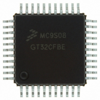
MC9S08GT32CFDE Freescale Semiconductor, MC9S08GT32CFDE Datasheet - Page 86

MC9S08GT32CFDE
Manufacturer Part Number
MC9S08GT32CFDE
Description
IC MCU 32K FLASH 20MHZ 48-QFN
Manufacturer
Freescale Semiconductor
Series
HCS08r
Specifications of MC9S08GT32CFDE
Core Processor
HCS08
Core Size
8-Bit
Speed
40MHz
Connectivity
I²C, SCI, SPI
Peripherals
LVD, POR, PWM, WDT
Number Of I /o
39
Program Memory Size
32KB (32K x 8)
Program Memory Type
FLASH
Ram Size
2K x 8
Voltage - Supply (vcc/vdd)
1.8 V ~ 3.6 V
Data Converters
A/D 8x10b
Oscillator Type
Internal
Operating Temperature
-40°C ~ 85°C
Package / Case
48-QFN
Controller Family/series
HCS08
No. Of I/o's
39
Ram Memory Size
2KB
Cpu Speed
40MHz
No. Of Timers
2
Rohs Compliant
Yes
For Use With
M68DEMO908GB60E - BOARD DEMO MC9S08GB60M68EVB908GB60E - BOARD EVAL FOR MC9S08GB60
Lead Free Status / RoHS Status
Lead free / RoHS Compliant
Eeprom Size
-
- Current page: 86 of 290
- Download datasheet (2Mb)
Chapter 6 Parallel Input/Output
PTASEn — Slew Rate Control Enable for Port A Bit n (n = 0–7)
PTADDn — Data Direction for Port A Bit n (n = 0–7)
6.6.2
Port B includes eight general-purpose I/O pins that share with the ATD function. Port B pins used as
general-purpose I/O pins are controlled by the port B data (PTBD), data direction (PTBDD), pullup enable
(PTBPE), and slew rate control (PTBSE) registers.
If the ATD takes control of a port B pin, the corresponding PTBDD, PTBSE, and PTBPE bits are ignored.
When a port B pin is being used as an ATD pin, reads of PTBD will return a 0 of the corresponding pin,
provided PTBDD is 0.
86
For port A pins that are outputs, these read/write control bits determine whether the slew rate
controlled outputs are enabled. For port A pins that are configured as inputs, these bits are ignored.
These read/write bits control the direction of port A pins and what is read for PTAD reads.
PTBD
PTBPE
PTBSE
PTBDD
1 = Slew rate control enabled.
0 = Slew rate control disabled.
1 = Output driver enabled for port A bit n and PTAD reads return the contents of PTADn.
0 = Input (output driver disabled) and reads return the pin value.
Port B Registers (PTBD, PTBPE, PTBSE, and PTBDD)
Reset:
Reset:
Reset:
Reset:
Read:
Write:
Read:
Write:
Read:
Write:
Read:
Write:
PTBPE7
PTBSE7
PTBDD7
PTBD7
Bit 7
0
0
0
0
PTBPE6
PTBSE6
PTBDD6
MC9S08GB/GT Data Sheet, Rev. 2.3
PTBD6
Figure 6-10. Port B Registers
6
0
0
0
0
PTBDD5
PTBPE5
PTBSE5
PTBD5
5
0
0
0
0
PTBDD4
PTBPE4
PTBSE4
PTBD4
4
0
0
0
0
PTBDD3
PTBPE3
PTBSE3
PTBD3
3
0
0
0
0
PTBDD2
PTBPE2
PTBSE2
PTBD2
2
0
0
0
0
PTBDD1
PTBPE1
PTBSE1
PTBD1
Freescale Semiconductor
1
0
0
0
0
PTBDD0
PTBPE0
PTBSE0
PTBD0
Bit 0
0
0
0
0
Related parts for MC9S08GT32CFDE
Image
Part Number
Description
Manufacturer
Datasheet
Request
R
Part Number:
Description:
Manufacturer:
Freescale Semiconductor, Inc
Datasheet:
Part Number:
Description:
Manufacturer:
Freescale Semiconductor, Inc
Datasheet:
Part Number:
Description:
Manufacturer:
Freescale Semiconductor, Inc
Datasheet:
Part Number:
Description:
Manufacturer:
Freescale Semiconductor, Inc
Datasheet:
Part Number:
Description:
Manufacturer:
Freescale Semiconductor, Inc
Datasheet:
Part Number:
Description:
Manufacturer:
Freescale Semiconductor, Inc
Datasheet:
Part Number:
Description:
Manufacturer:
Freescale Semiconductor, Inc
Datasheet:
Part Number:
Description:
Manufacturer:
Freescale Semiconductor, Inc
Datasheet:
Part Number:
Description:
Manufacturer:
Freescale Semiconductor, Inc
Datasheet:
Part Number:
Description:
Manufacturer:
Freescale Semiconductor, Inc
Datasheet:
Part Number:
Description:
Manufacturer:
Freescale Semiconductor, Inc
Datasheet:
Part Number:
Description:
Manufacturer:
Freescale Semiconductor, Inc
Datasheet:
Part Number:
Description:
Manufacturer:
Freescale Semiconductor, Inc
Datasheet:
Part Number:
Description:
Manufacturer:
Freescale Semiconductor, Inc
Datasheet:
Part Number:
Description:
Manufacturer:
Freescale Semiconductor, Inc
Datasheet:


