MC9S08GT32CFDE Freescale Semiconductor, MC9S08GT32CFDE Datasheet - Page 198
MC9S08GT32CFDE
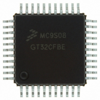
Manufacturer Part Number
MC9S08GT32CFDE
Description
IC MCU 32K FLASH 20MHZ 48-QFN
Manufacturer
Freescale Semiconductor
Series
HCS08r
Specifications of MC9S08GT32CFDE
Core Processor
HCS08
Core Size
8-Bit
Speed
40MHz
Connectivity
I²C, SCI, SPI
Peripherals
LVD, POR, PWM, WDT
Number Of I /o
39
Program Memory Size
32KB (32K x 8)
Program Memory Type
FLASH
Ram Size
2K x 8
Voltage - Supply (vcc/vdd)
1.8 V ~ 3.6 V
Data Converters
A/D 8x10b
Oscillator Type
Internal
Operating Temperature
-40°C ~ 85°C
Package / Case
48-QFN
Controller Family/series
HCS08
No. Of I/o's
39
Ram Memory Size
2KB
Cpu Speed
40MHz
No. Of Timers
2
Rohs Compliant
Yes
For Use With
M68DEMO908GB60E - BOARD DEMO MC9S08GB60M68EVB908GB60E - BOARD EVAL FOR MC9S08GB60
Lead Free Status / RoHS Status
Lead free / RoHS Compliant
Eeprom Size
-


Serial Peripheral Interface (SPI) Module
SSOE — Slave Select Output Enable
LSBFE — LSB First (Shifter Direction)
12.4.2
This read/write register is used to control optional features of the SPI system. Bits 7, 6, 5, and 2 are not
implemented and always read 0.
MODFEN — Master Mode-Fault Function Enable
198
This bit is used in combination with the mode fault enable (MODFEN) bit in SPCR2 and the
master/slave (MSTR) control bit to determine the function of the SS1 pin as shown in
When the SPI is configured for slave mode, this bit has no meaning or effect. (The SS1 pin is the slave
select input.) In master mode, this bit determines how the SS1 pin is used (refer to
details).
1 = SPI serial data transfers start with least significant bit.
0 = SPI serial data transfers start with most significant bit.
1 = Mode fault function enabled, master SS1 pin acts as the mode fault input or the slave select
0 = Mode fault function disabled, master SS1 pin reverts to general-purpose I/O not controlled by
SPI Control Register 2 (SPI1C2)
output.
SPI.
MODFEN
0
0
1
1
Reset:
Read:
Write:
SSOE
0
1
0
1
Bit 7
Figure 12-8. SPI Control Register 2 (SPI1C2)
0
0
General-purpose I/O (not SPI)
General-purpose I/O (not SPI)
SS input for mode fault
Automatic SS output
= Unimplemented or Reserved
MC9S08GB/GT Data Sheet, Rev. 2.3
Table 12-1. SS1 Pin Function
6
0
0
Master Mode
5
0
0
MODFEN BIDIROE
4
0
Slave select input
Slave select input
Slave select input
Slave select input
3
0
Slave Mode
2
0
0
SPISWAI
Freescale Semiconductor
Table 12-1
1
0
Table
SPC0
Bit 0
0
for more
12-1.
Related parts for MC9S08GT32CFDE
Image
Part Number
Description
Manufacturer
Datasheet
Request
R

Part Number:
Description:
Manufacturer:
Freescale Semiconductor, Inc
Datasheet:
Part Number:
Description:
Manufacturer:
Freescale Semiconductor, Inc
Datasheet:
Part Number:
Description:
Manufacturer:
Freescale Semiconductor, Inc
Datasheet:
Part Number:
Description:
Manufacturer:
Freescale Semiconductor, Inc
Datasheet:
Part Number:
Description:
Manufacturer:
Freescale Semiconductor, Inc
Datasheet:
Part Number:
Description:
Manufacturer:
Freescale Semiconductor, Inc
Datasheet:
Part Number:
Description:
Manufacturer:
Freescale Semiconductor, Inc
Datasheet:
Part Number:
Description:
Manufacturer:
Freescale Semiconductor, Inc
Datasheet:
Part Number:
Description:
Manufacturer:
Freescale Semiconductor, Inc
Datasheet:
Part Number:
Description:
Manufacturer:
Freescale Semiconductor, Inc
Datasheet:
Part Number:
Description:
Manufacturer:
Freescale Semiconductor, Inc
Datasheet:
Part Number:
Description:
Manufacturer:
Freescale Semiconductor, Inc
Datasheet:
Part Number:
Description:
Manufacturer:
Freescale Semiconductor, Inc
Datasheet:
Part Number:
Description:
Manufacturer:
Freescale Semiconductor, Inc
Datasheet:
Part Number:
Description:
Manufacturer:
Freescale Semiconductor, Inc
Datasheet: