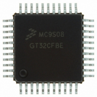
MC9S08GT32CFDE Freescale Semiconductor, MC9S08GT32CFDE Datasheet - Page 147

MC9S08GT32CFDE
Manufacturer Part Number
MC9S08GT32CFDE
Description
IC MCU 32K FLASH 20MHZ 48-QFN
Manufacturer
Freescale Semiconductor
Series
HCS08r
Specifications of MC9S08GT32CFDE
Core Processor
HCS08
Core Size
8-Bit
Speed
40MHz
Connectivity
I²C, SCI, SPI
Peripherals
LVD, POR, PWM, WDT
Number Of I /o
39
Program Memory Size
32KB (32K x 8)
Program Memory Type
FLASH
Ram Size
2K x 8
Voltage - Supply (vcc/vdd)
1.8 V ~ 3.6 V
Data Converters
A/D 8x10b
Oscillator Type
Internal
Operating Temperature
-40°C ~ 85°C
Package / Case
48-QFN
Controller Family/series
HCS08
No. Of I/o's
39
Ram Memory Size
2KB
Cpu Speed
40MHz
No. Of Timers
2
Rohs Compliant
Yes
For Use With
M68DEMO908GB60E - BOARD DEMO MC9S08GB60M68EVB908GB60E - BOARD EVAL FOR MC9S08GB60
Lead Free Status / RoHS Status
Lead free / RoHS Compliant
Eeprom Size
-
- Current page: 147 of 290
- Download datasheet (2Mb)
9.3
Figure 9-3
The KBI module allows up to eight pins to act as additional interrupt sources. Four of these pins allow
falling-edge sensing while the other four can be configured for either rising-edge sensing or falling-edge
sensing. The sensing mode for all eight pins can also be modified to detect edges and levels instead of only
edges.
9.4
This on-chip peripheral module is called a keyboard interrupt (KBI) module because originally it was
designed to simplify the connection and use of row-column matrices of keyboard switches. However, these
inputs are also useful as extra external interrupt inputs and as an external means of waking up the MCU
from stop or wait low-power modes.
9.4.1
The KBIPEn control bits in the KBI1PE register allow a user to enable (KBIPEn = 1) any combination of
KBI-related port pins to be connected to the KBI module. Pins corresponding to 0s in KBI1PE are
general-purpose I/O pins that are not associated with the KBI module.
9.4.2
Synchronous logic is used to detect edges. Prior to detecting an edge, enabled keyboard inputs in a KBI
module must be at the deasserted logic level.
A falling edge is detected when an enabled keyboard input signal is seen as a logic 1 (the deasserted level)
during one bus cycle and then a logic 0 (the asserted level) during the next cycle.
Freescale Semiconductor
KBI1P0
KBI1P3
KBI1P4
KBI1Pn
KBEDGn
KBEDG4
KBI Block Diagram
Keyboard Interrupt (KBI) Module
shows the block diagram for a KBI module.
Pin Enables
Edge and Level Sensitivity
0
1
0
1
S
S
KBIPE0
KBIPE3
KBIPE4
KBIPEn
MC9S08GB/GT Data Sheet, Rev. 2.3
Figure 9-3. KBI Block Diagram
KBIMOD
V
DD
D
CK
CLR
Q
INTERRUPT FF
KEYBOARD
KBACK
RESET
STOP
SYNCHRONIZER
BUSCLK
STOP BYPASS
KBIE
KBI Block Diagram
KBF
KEYBOARD
INTERRUPT
REQUEST
147
Related parts for MC9S08GT32CFDE
Image
Part Number
Description
Manufacturer
Datasheet
Request
R
Part Number:
Description:
Manufacturer:
Freescale Semiconductor, Inc
Datasheet:
Part Number:
Description:
Manufacturer:
Freescale Semiconductor, Inc
Datasheet:
Part Number:
Description:
Manufacturer:
Freescale Semiconductor, Inc
Datasheet:
Part Number:
Description:
Manufacturer:
Freescale Semiconductor, Inc
Datasheet:
Part Number:
Description:
Manufacturer:
Freescale Semiconductor, Inc
Datasheet:
Part Number:
Description:
Manufacturer:
Freescale Semiconductor, Inc
Datasheet:
Part Number:
Description:
Manufacturer:
Freescale Semiconductor, Inc
Datasheet:
Part Number:
Description:
Manufacturer:
Freescale Semiconductor, Inc
Datasheet:
Part Number:
Description:
Manufacturer:
Freescale Semiconductor, Inc
Datasheet:
Part Number:
Description:
Manufacturer:
Freescale Semiconductor, Inc
Datasheet:
Part Number:
Description:
Manufacturer:
Freescale Semiconductor, Inc
Datasheet:
Part Number:
Description:
Manufacturer:
Freescale Semiconductor, Inc
Datasheet:
Part Number:
Description:
Manufacturer:
Freescale Semiconductor, Inc
Datasheet:
Part Number:
Description:
Manufacturer:
Freescale Semiconductor, Inc
Datasheet:
Part Number:
Description:
Manufacturer:
Freescale Semiconductor, Inc
Datasheet:


