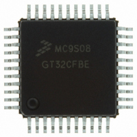
MC9S08GT32CFDE Freescale Semiconductor, MC9S08GT32CFDE Datasheet - Page 46

MC9S08GT32CFDE
Manufacturer Part Number
MC9S08GT32CFDE
Description
IC MCU 32K FLASH 20MHZ 48-QFN
Manufacturer
Freescale Semiconductor
Series
HCS08r
Specifications of MC9S08GT32CFDE
Core Processor
HCS08
Core Size
8-Bit
Speed
40MHz
Connectivity
I²C, SCI, SPI
Peripherals
LVD, POR, PWM, WDT
Number Of I /o
39
Program Memory Size
32KB (32K x 8)
Program Memory Type
FLASH
Ram Size
2K x 8
Voltage - Supply (vcc/vdd)
1.8 V ~ 3.6 V
Data Converters
A/D 8x10b
Oscillator Type
Internal
Operating Temperature
-40°C ~ 85°C
Package / Case
48-QFN
Controller Family/series
HCS08
No. Of I/o's
39
Ram Memory Size
2KB
Cpu Speed
40MHz
No. Of Timers
2
Rohs Compliant
Yes
For Use With
M68DEMO908GB60E - BOARD DEMO MC9S08GB60M68EVB908GB60E - BOARD EVAL FOR MC9S08GB60
Lead Free Status / RoHS Status
Lead free / RoHS Compliant
Eeprom Size
-
- Current page: 46 of 290
- Download datasheet (2Mb)
1
$FFB0 –
$FFB7
$FFB8 –
$FFBC
$FFBD
$FFBE
$FFBF
Chapter 4 Memory
Provided the key enable (KEYEN) bit is 1, the 8-byte comparison key can be used to temporarily
disengage memory security. This key mechanism can be accessed only through user code running in secure
memory. (A security key cannot be entered directly through background debug commands.) This security
key can be disabled completely by programming the KEYEN bit to 0. If the security key is disabled, the
only way to disengage security is by mass erasing the FLASH if needed (normally through the background
debug interface) and verifying that FLASH is blank. To avoid returning to secure mode after the next reset,
program the security bits (SEC01:SEC00) to the unsecured state (1:0).
4.3
The MC9S08GB/GT includes static RAM. The locations in RAM below $0100 can be accessed using the
more efficient direct addressing mode, and any single bit in this area can be accessed with the bit
manipulation instructions (BCLR, BSET, BRCLR, and BRSET). Locating the most frequently accessed
program variables in this area of RAM is preferred.
The RAM retains data when the MCU is in low-power wait, stop2, or stop3 mode. At power-on or after
wakeup from stop1, the contents of RAM are uninitialized. RAM data is unaffected by any reset provided
that the supply voltage does not drop below the minimum value for RAM retention.
For compatibility with older M68HC05 MCUs, the HCS08 resets the stack pointer to $00FF. In the
MC9S08GB/GT, it is usually best to re-initialize the stack pointer to the top of the RAM so the direct page
RAM can be used for frequently accessed RAM variables and bit-addressable program variables. Include
the following 2-instruction sequence in your reset initialization routine (where RamLast is equated to the
highest address of the RAM in the Freescale-provided equate file).
When security is enabled, the RAM is considered a secure memory resource and is not accessible through
BDM or through code executing from non-secure memory. See
description of the security feature.
4.4
The FLASH memory is intended primarily for program storage. In-circuit programming allows the
operating program to be loaded into the FLASH memory after final assembly of the application product.
46
Address
This location is used to store the factory trim value for the ICG.
NVBACKKEY
Reserved
NVPROT
Reserved
NVOPT
RAM
FLASH
Register Name
LDHX
TXS
1
#RamLast+1
FPOPEN
KEYEN
Bit 7
—
—
—
Table 4-4. Nonvolatile Register Summary
FNORED
MC9S08GB/GT Data Sheet, Rev. 2.3
FPDIS
—
—
—
6
;point one past RAM
;SP<-(H:X-1)
FPS2
—
—
—
5
0
8-Byte Comparison Key
FPS1
—
—
—
4
0
Section 4.5,
FPS0
—
—
—
3
0
“Security”
—
—
—
2
0
0
Freescale Semiconductor
SEC01
for a detailed
—
—
—
1
0
SEC00
Bit 0
—
—
—
0
Related parts for MC9S08GT32CFDE
Image
Part Number
Description
Manufacturer
Datasheet
Request
R
Part Number:
Description:
Manufacturer:
Freescale Semiconductor, Inc
Datasheet:
Part Number:
Description:
Manufacturer:
Freescale Semiconductor, Inc
Datasheet:
Part Number:
Description:
Manufacturer:
Freescale Semiconductor, Inc
Datasheet:
Part Number:
Description:
Manufacturer:
Freescale Semiconductor, Inc
Datasheet:
Part Number:
Description:
Manufacturer:
Freescale Semiconductor, Inc
Datasheet:
Part Number:
Description:
Manufacturer:
Freescale Semiconductor, Inc
Datasheet:
Part Number:
Description:
Manufacturer:
Freescale Semiconductor, Inc
Datasheet:
Part Number:
Description:
Manufacturer:
Freescale Semiconductor, Inc
Datasheet:
Part Number:
Description:
Manufacturer:
Freescale Semiconductor, Inc
Datasheet:
Part Number:
Description:
Manufacturer:
Freescale Semiconductor, Inc
Datasheet:
Part Number:
Description:
Manufacturer:
Freescale Semiconductor, Inc
Datasheet:
Part Number:
Description:
Manufacturer:
Freescale Semiconductor, Inc
Datasheet:
Part Number:
Description:
Manufacturer:
Freescale Semiconductor, Inc
Datasheet:
Part Number:
Description:
Manufacturer:
Freescale Semiconductor, Inc
Datasheet:
Part Number:
Description:
Manufacturer:
Freescale Semiconductor, Inc
Datasheet:


